IXFN200N10P IXYS SEMICONDUCTOR, IXFN200N10P Datasheet
IXFN200N10P
Manufacturer Part Number
IXFN200N10P
Description
MOSFET, N, SOT-227B
Manufacturer
IXYS SEMICONDUCTOR
Datasheet
1.IXFN200N10P.pdf
(5 pages)
Specifications of IXFN200N10P
Transistor Polarity
N Channel
Continuous Drain Current Id
200A
Drain Source Voltage Vds
100V
On Resistance Rds(on)
7.5mohm
Rds(on) Test Voltage Vgs
15V
Voltage Vgs Max
20V
Operating Temperature Range
-55°C
Threshold Voltage Vgs Typ
5V
Rohs Compliant
Yes
Lead Free Status / RoHS Status
Lead free / RoHS Compliant
Available stocks
Company
Part Number
Manufacturer
Quantity
Price
Company:

Part Number:
IXFN200N10P
Manufacturer:
KEMET
Quantity:
30 000
Part Number:
IXFN200N10P
Quantity:
129


Polar
Power MOSFET
N-Channel Enhancement Mode
Fast Intrinsic Diode
Avalanche Rated
Symbol
V
V
V
V
I
I
I
I
E
E
dv/dt
P
T
T
T
V
M
Weight
Symbol
(T
BV
V
I
I
R
D25
D(RMS)
DM
AR
GSS
DSS
J
JM
stg
© 2006 IXYS All rights reserved
DSS
DGR
GS
GSM
AR
AS
D
ISOL
GS(th)
DS(on)
d
J
DSS
= 25°C, unless otherwise specified)
TM
Test Conditions
T
T
Continuous
Transient
T
External lead current limit
T
T
T
T
I
T
T
50/60 Hz, RMS,
I
Mounting torque, Terminal connection torque
Test Conditions
V
V
V
V
V
V
Pulse test, t ≤ 300 μs, duty cycle d ≤ 2 %
S
ISOL
J
J
C
C
C
C
C
J
C
GS
DS
GS
DS
GS
GS
HiPerFET
= 25°C to 175°C
= 25°C to 175°C; R
= 25°C
= 25°C, pulse width limited by T
= 25°C
= 25°C
= 25°C
≤ I
≤ 150°C, R
= 25°C
≤ 1 mA,
= 0 V, I
= V
= ±20 V, V
= V
= 10 V, I
= 15 V, I
DM
, di/dt ≤ 100 A/μs, V
GS
DSS,
, I
D
D
V
D
D
= 250 μA
= 8 mA
GS
G
= 0.5 I
= 400A
DS
= 0 V
= 4 Ω
= 0
D25
GS
= 1 MΩ
DD
T
T
≤ V
J
J
= 150°C
= 175°C
IXFN 200N10P
T = 1 min
T = 1 s
DSS
JM
,
100
Min.
3.0
Characteristic Values
-55 ... +175
-55 ... +150
Maximum Ratings
Typ.
5.5
1.5/13
2500
3000
100
100
±20
±30
200
100
400
100
680
175
60
10
30
4
±100
500
Max.
5.0
2.5
7.5
25
lb.in.
V/ns
mΩ
mΩ
mA
mJ
V~
V~
nA
μA
μA
°C
°C
°C
W
V
V
V
V
A
A
A
A
V
V
g
J
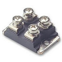
miniBLOC, SOT-227 B (IXFN)
G = Gate
S = Source
Either Source terminal S can be used as the
Source terminal or the Kelvin Source (gate
return) terminal.
Features
•
•
•
•
•
•
•
•
Applications
•
•
•
•
•
•
•
Advantages
•
•
•
International standard package
Encapsulating epoxy meets
UL 94 V-0, flammability classification
miniBLOC with Aluminium nitride
isolation
Low R
Rugged polysilicon gate cell structure
Unclamped Inductive Switching (UIS)
rated
Low package inductance
Fast intrinsic Rectifier
DC-DC converters
Synchronous rectification
Battery chargers
Switched-mode and resonant-mode
power supplies
DC choppers
Temperature and lighting controls
Low voltage relays
Easy to mount
Space savings
High power density
V
I
R
t
E153432
D25
rr
DS (on)
DS(on)
DSS
G
HDMOS
S
D = Drain
= 100 V
= 200 A
≤ ≤ ≤ ≤ ≤ 7.5 mΩ Ω Ω Ω Ω
≤ ≤ ≤ ≤ ≤ 150 ns
D
TM
process
DS99239E(03/06)
S
Related parts for IXFN200N10P
Image
Part Number
Description
Manufacturer
Datasheet
Request
R

Part Number:
Description:
Hiperfettm Power Mosfets Ixfn 26n90 Single Die Mosfet Ixfn 25n90 N-channel Enhancement Mode Avalanche Rated, High Dv/dt, Low Trr
Manufacturer:
IXYS Corporation
Datasheet:

Part Number:
Description:
HiPerFETTM Power MOSFETs Single Die MOSFET
Manufacturer:
IXYS [IXYS Corporation]
Datasheet:

Part Number:
Description:
Discrete Semiconductor Modules 1000 Amps 100V
Manufacturer:
IXYS
Datasheet:
Part Number:
Description:
Discrete Semiconductor Modules 300 Amps 1200V
Manufacturer:
IXYS
Datasheet:
Part Number:
Description:
Discrete Semiconductor Modules 450 Amps 1200V
Manufacturer:
IXYS
Datasheet:
Part Number:
Description:
Discrete Semiconductor Modules
Manufacturer:
IXYS
Datasheet:
Part Number:
Description:
Discrete Semiconductor Modules 1500 Amps 75V
Manufacturer:
IXYS
Datasheet:
Part Number:
Description:
Discrete Semiconductor Modules 300 Amps 1200V
Manufacturer:
IXYS
Datasheet:
Part Number:
Description:
Discrete Semiconductor Modules 225 Amps 1200V
Manufacturer:
IXYS
Datasheet:

Part Number:
Description:
DIODE MODULE EPITAXIAL 600V 95A
Manufacturer:
IXYS
Datasheet:

Part Number:
Description:
MODULE IGBT CBI E1
Manufacturer:
IXYS
Datasheet:

Part Number:
Description:
MODULE IGBT CBI E2
Manufacturer:
IXYS
Datasheet:

Part Number:
Description:
MOSFET N-CH 100V 1245A Y3-LI
Manufacturer:
IXYS
Datasheet:

Part Number:
Description:
THYRISTOR DIODE MODULE
Manufacturer:
IXYS
Datasheet:
IXFN200N10P Summary of contents
Page 1
TM Polar HiPerFET Power MOSFET N-Channel Enhancement Mode Fast Intrinsic Diode Avalanche Rated Symbol Test Conditions 25°C to 175°C DSS 25°C to 175°C; R DGR J V Continuous GS V Transient GSM I ...
Page 2
Symbol Test Conditions 0 D25 C iss MHz oss rss t d(on ...
Page 3
Fig. 1. Output Characte r is tics º 200 V = 10V GS 175 9V 150 125 100 0.2 0.4 0.6 0 olts D S Fig. 3. Output Characte r ...
Page 4
Fig. 7. Input Adm ittance 300 250 200 150 º 150 C 100 J º º - 4.5 5 5 olts G S Fig. 9. Sour ce ...
Page 5
Fig. 13. Maximum Transient Thermal Resistance 1.000 0.100 0.010 0.001 0.00001 0.0001 © 2006 IXYS All rights reserved 0.001 0.01 Pulse Width - Seconds IXFN 200N10P 0 IXYS REF: T_200N10P (88) 03-22-06-E.xls ...