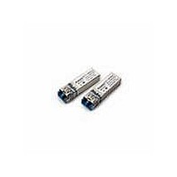
HFCT-5953TL Avago Technologies US Inc., HFCT-5953TL Datasheet - Page 6

HFCT-5953TL
Manufacturer Part Number
HFCT-5953TL
Description
Fiber Optic Transmitters, Receivers, Transceivers OC12 IR 2x5 SFF LC
Manufacturer
Avago Technologies US Inc.
Datasheet
1.HFCT-5953TL.pdf
(17 pages)
Specifications of HFCT-5953TL
Function
High performance, modules for serial optical data communication applications, designed for single mode fiber.
Product
Transceiver
Data Rate
622 Mbps
Wavelength
1300 nm
Maximum Rise Time
1 ns, 0.5 ns
Maximum Fall Time
1 ns, 0.5 ns
Maximum Output Current
50 mA
Operating Supply Voltage
3.14 V to 3.47 V
Maximum Operating Temperature
+ 70 C
Minimum Operating Temperature
0 C
Package / Case
DIP-10 with Connector
Optical Fiber Type
TX/RX
Data Transfer Rate
622Mbps
Optical Rise Time
1/0.5ns
Optical Fall Time
1/0.5ns
Operating Temperature Classification
Commercial
Peak Wavelength
1356/1570nm
Package Type
DIP With Connector
Operating Supply Voltage (min)
3.14V
Operating Supply Voltage (typ)
3.3V
Operating Supply Voltage (max)
3.47V
Output Current
50mA
Operating Temp Range
0C to 70C
Mounting
Snap Fit To Panel
Pin Count
10
For Use With
Singlemode Glass
Lead Free Status / RoHS Status
Lead free / RoHS Compliant
RECEIVER DATA OUTPUT BAR
6
Connection Diagram (HFCT-5954xxx)
Figure 5 - Pin Out Diagram (Top View)
Pin Descriptions:
Pin 1 Photo Detector Bias, VpdR:
Pin 1 must be connected to VCC for the receiver to work.
This pin enables monitoring of photo detector bias current. It
must be connected directly to V
a resistor (Max 200 R) for monitoring photo detector
bias current.
Pins 2, 3, 6 Receiver Signal Ground V
Directly connect these pins to the receiver ground plane.
Pins 4, 5 DO NOT CONNECT
Pin 7 Receiver Power Supply V
Provide +3.3 V dc via the recommended receiver power sup-
ply filter circuit. Locate the power supply filter circuit as close
as possible to the V
not cause V
Pin 8 Signal Detect SD:
Normal optical input levels to the receiver result in a logic “1”
output. Low optical input levels to the receiver result in a logic
“0” output. This Signal Detect output can be used to drive a
low voltage TTL input on an upstream circuit, such as Signal
Detect input or Loss of Signal-bar.
Pin 9 Receiver Data Out Bar RD-:
No internal terminations are provided. See recommended
circuit schematic.
Pin 10 Receiver Data Out RD+:
No internal terminations are provided. See recommended
circuit schematic.
Pin 11 Transmitter Power Supply V
Provide +3.3 V dc via the recommended transmitter power
supply filter circuit. Locate the power supply filter circuit as
close as possible to the V
Pins 12, 16 Transmitter Signal Ground V
Directly connect these pins to the transmitter signal ground
plane.
RECEIVER SIGNAL GROUND
RECEIVER SIGNAL GROUND
RECEIVER SIGNAL GROUND
RECEIVER POWER SUPPLY
RECEIVER DATA OUTPUT
PHOTO DETECTOR BIAS
Grounding Tabs
NOT CONNECTED
NOT CONNECTED
SIGNAL DETECT
Package
CC
to drop below minimum specification.
CC
RX pin. Note: the filter circuit should
o
o
o
o
o
o
o
o
o
o
RX
10
1
2
3
4
5
6
7
8
9
View
CC
Top
TX pin.
CC
TX
20
19
18
17
16
15
14
13
12
11
RX:
o
o
o
o
o
o
o
o
o
o
CC
CC
EE
TX:
RX, or to V
LASER DIODE OPTICAL POWER MONITOR - POSITIVE END
LASER DIODE OPTICAL POWER MONITOR - NEGATIVE END
LASER DIODE BIAS CURRENT MONITOR - POSITIVE END
LASER DIODE BIAS CURRENT MONITOR - NEGATIVE END
TRANSMITTER SIGNAL GROUND
TRANSMITTER DATA IN BAR
TRANSMITTER DATA IN
TRANSMITTER DISABLE
TRANSMITTER SIGNAL GROUND
TRANSMITTER POWER SUPPLY
RX:
EE
Mounting Studs/
TX:
Solder Posts
CC
RX through
Pin 13 Transmitter Disable T
Optional feature, connect this pin to +3.3 V TTL logic high “1”
to disable module. To enable module connect to TTL logic
low “0”.
Pin 14 Transmitter Data In TD+:
No internal terminations are provided. See recommended
circuit schematic.
Pin 15 Transmitter Data In Bar TD-:
No internal terminations are provided. See recommended
circuit schematic.
Pin 17 Laser Diode Bias Current Monitor - Negative End B
The laser diode bias current is accessible by measuring the
voltage developed across pins 17 and 18. Dividing the volt-
age by 10 Ohms (internal) will yield the value of the laser bias
current.
Pin 18 Laser Diode Bias Current Monitor - Positive End B
See pin 17 description.
Pin 19 Laser Diode Optical Power Monitor - Negative End P
The back facet diode monitor current is accessible by measur-
ing the voltage developed across pins 19 and 20. The voltage
across a 200 Ohm internal resistor between pins 19 and 20
will be proportional to the photo current.
Pin 20 Laser Diode Optical Power Monitor - Positive End P
See pin 19 description.
Mounting Studs/Solder Posts
The two mounting studs are provided for transceiver me-
chanical attachment to the circuit board. It is recommended
that the holes in the circuit board be connected to chassis
ground.
Package Grounding Tabs
Connect four package grounding tabs to signal ground.
DIS
:
MON
MON
MON
MON
+
–
+
–


