HFBR-7924 Avago Technologies US Inc., HFBR-7924 Datasheet - Page 6
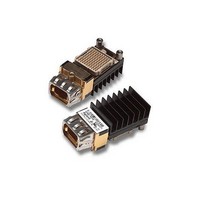
HFBR-7924
Manufacturer Part Number
HFBR-7924
Description
Fiber Optic Transmitters, Receivers, Transceivers 4+4 2.7Gbps Pluggabl e Txcvr Module
Manufacturer
Avago Technologies US Inc.
Datasheet
1.HFBR-7924.pdf
(18 pages)
Specifications of HFBR-7924
Function
Pluggable Transceiver, for Parallel Optics
Product
Transceiver
Wavelength
850 nm
Maximum Rise Time
150 ps
Maximum Fall Time
150 ps
Pulse Width Distortion
0.045 ns
Maximum Output Current
25 mA
Operating Supply Voltage
3.135 V to 3.465 V
Maximum Operating Temperature
+ 80 C
Minimum Operating Temperature
0 C
Optical Fiber Type
TX/RX
Data Transfer Rate
2700MBd
Optical Rise Time
0.15ns
Optical Fall Time
0.15ns
Jitter
0.045ns
Operating Temperature Classification
Commercial
Peak Wavelength
850/860nm
Operating Supply Voltage (min)
3.135V
Operating Supply Voltage (typ)
3.3V
Operating Supply Voltage (max)
3.465V
Output Current
25mA
Operating Temp Range
0C to 80C
Mounting
Screw
Pin Count
100
For Use With
Multimode Glass
Lead Free Status / RoHS Status
Lead free / RoHS Compliant


Absolute Maximum Ratings
Stresses in excess of the absolute maximum ratings can cause catastrophic damage to the device. Limits apply to each
parameter in isolation, all other parameters having values within the recommended operating conditions. It should not be
assumed that limiting values of more than one parameter can be applied to the product at the same time. Exposure to the
absolute maximum ratings for extended periods can adversely affect device reliability.
Recommended Operating Conditions
Recommended Operating Conditions specify conditions for which the optical and electrical characteristics hold. Optical and
electrical characteristics are not specified for operation beyond the Recommended Operating Conditions, reliability is not
implied and damage to the device may occur for such operation over an extended time period.
Notes:
1. This is the maximum voltage that can be applied across the Transmitter Differential Data Inputs without damaging the input circuit.
2. Case Temperature is measured as indicated in Figure 2.
3. Data inputs are CML compatible. Coupling capacitors are required to block dc. ∆V
4. Power Supply Noise is defined at the supply side of the recommended filter for all V
5. For data patterns with restricted run lengths, e.g. 8B10B encoded data, smaller value capacitors may provide acceptable results.
Parameter
Data/Control Signal Input Voltage
Relative Humidity (Non Condensing)
Parameter
Data Input Differential Peak-to-Peak
Data Input Rise & Fall Time (20-80%)
Power Supply Noise
Data I/O Coupling Capacitors
Receiver Differential Data Output Load
6
Storage Temperature
Supply Voltage
Transmitter Differential Input Voltage
Output Current (dc)
Case Temperature
Supply Voltage
Signaling Rate/Channel
Voltage Swing
Control Input Voltage High
Control Input Voltage Low
Differential Data Input Voltage and ∆V
2700 MHz with the recommended power supply filter in place.
DINL
= Low State Differential Data Input Voltage.
| V
Symbol
I
RH
Symbol
N
C
R
T
V
V
T
V
DV
t
V
V
D
r
S
C
, t
AC
DL
CC
I
CC
IH
IL
P
D
DINP-P
f
|
Minimum
Minimum Typical
1
175
-40
-0.5
-0.5
5
0
3.135
2.0
V
EE
3.3
0.1
100
DIN p-p
CC
Maximum
+100
4.6
2
25
95
V
CC
supplies over the frequency range from 500 Hz to
+ 0.5
= ∆V
Maximum Unit
+80
3.465
2.7
1600
160
0.8
200
V
CC
DINH
- ∆V
DINL
Unit
ºC
mA
%
GBd
mV
ps
mV
µF
V
V
V
ºC
V
V
V
W
, where ∆V
P-P
P-P
Reference
1
Reference
2, Figures 2,
Figure 8
3, Figures 11,12
4, Figure 8
5, Figure 9
Figure 9
DINH
= High State
Related parts for HFBR-7924
Image
Part Number
Description
Manufacturer
Datasheet
Request
R

Part Number:
Description:
RECEIVER FIBER OPTIC 600NM 5MBD
Manufacturer:
Avago Technologies US Inc.
Datasheet:

Part Number:
Description:
RECEIVER FIBER OPTIC 600NM 40KBD
Manufacturer:
Avago Technologies US Inc.
Datasheet:

Part Number:
Description:
RCVR FIBER OPTIC INTERBUS-S
Manufacturer:
Avago Technologies US Inc.
Datasheet:

Part Number:
Description:
RCVR OPT HI PERF VERS LINK HORZ
Manufacturer:
Avago Technologies US Inc.
Datasheet:
Part Number:
Description:
RCVR OPT HI PERF VERS LINK HORZ
Manufacturer:
Avago Technologies US Inc.
Datasheet:

Part Number:
Description:
XMITTER FIBER OPTIC 600NM 5MBD
Manufacturer:
Avago Technologies US Inc.
Datasheet:

Part Number:
Description:
XMITTER FIBER OPTIC 600NM 40KBD
Manufacturer:
Avago Technologies US Inc.
Datasheet:

Part Number:
Description:
XMITTER FIBER OPTIC HIGH PWR ST
Manufacturer:
Avago Technologies US Inc.
Datasheet:
Part Number:
Description:
XMITTER VERSATILE LINK HORZ
Manufacturer:
Avago Technologies US Inc.
Datasheet:
Part Number:
Description:
XMITTER VERSATILE LINK HORZ
Manufacturer:
Avago Technologies US Inc.
Datasheet:

Part Number:
Description:
XMITTER OPT HI PERFORMANCE VERT
Manufacturer:
Avago Technologies US Inc.
Datasheet:

Part Number:
Description:
Fiber Optic Transmitters, Receivers, Transceivers Versatile Link Horiz
Manufacturer:
Avago Technologies US Inc.
Datasheet:
Part Number:
Description:
Fiber Optic Transmitters, Receivers, Transceivers Versatile Link Horiz
Manufacturer:
Avago Technologies US Inc.
Datasheet:
Part Number:
Description:
Fiber Optic Transmitters, Receivers, Transceivers Versatile Link Horiz
Manufacturer:
Avago Technologies US Inc.
Datasheet:

Part Number:
Description:
FIBER OPTIC TRANSMITTER 660NM
Manufacturer:
Avago Technologies US Inc.
Datasheet: