DLP-USB245M DLP Design Inc, DLP-USB245M Datasheet - Page 7
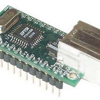
DLP-USB245M
Manufacturer Part Number
DLP-USB245M
Description
Interface Modules & Development Tools USB-FIFO Adapter
Manufacturer
DLP Design Inc
Datasheet
1.DLP-USB245M-G.pdf
(15 pages)
Specifications of DLP-USB245M
Interface Type
USB
Operating Supply Voltage
- 0.5 V to + 6 V
Product
Interface Modules
For Use With/related Products
FT245BM
Lead Free Status / RoHS Status
Lead free / RoHS Compliant


9
10
11
12
13
14
15
16
17
18
19
20
21
22
23
24
SND/WUP
initiates a remote wakeup sequence. If the device is active (not in suspend) a positive edge on this
pin (SEND) causes the data in the write buffer to be sent to the PC on the next USB Data-In request
regardless of how many bytes are in the buffer.
VCC-IO
When interfacing with 3.3v external logic connect VCC-IO to the 3.3v supply of the external logic,
otherwise connect to VCC to drive out at 5v CMOS level. This pin must be connected to VCC from
the target electronics or EXTVCC.
EXTVCC
PORTVCC if module is to be powered by the USB port (typical configuration)
PORTVCC
USB port (typical configuration). 500mA maximum current available to USB adapter and target
electronics if USB device is configured for high power.
RXF#
to be read with RD#. RXF# goes high when the receive buffer is empty.
TXE#
Do not attempt to write data to the transmit buffer when TXE# is high.
WR
the FIFO’s transmit buffer. Data written to the transmit buffer is sent to the host PC within the TX
buffer timeout value ( default 16mS ) and placed in the RS-232 buffer opened by the application
program. Note : The FT245BM allows the TX buffer timeout value to be reprogrammed to a value
between 1 and 255mS depending on the applicaton requirement, also the SND pin can be used to
send any remaining data in the TX buffer regardless of the timeout value.
RD#
byte in the FIFO’s receive buffer. Taking RD# high returns the data pins to a high impedance state
and prepares the next byte (if available) in the FIFO to be read.
D7
D6
D5
D4
D3
D2
D1
D0
I/O Bi-directional Data Bus Bit # 7
I/O Bi-directional Data Bus Bit # 6
I/O Bi-directional Data Bus Bit # 5
I/O Bi-directional Data Bus Bit # 4
I/O Bi-directional Data Bus Bit # 3
I/O Bi-directional Data Bus Bit # 2
I/O Bi-directional Data Bus Bit # 1
I/O Bi-directional Data Bus Bit # 0
Copyright © DLP Design 2002
(In) When taken from a high to a low state, WR reads the 8 data lines and writes the byte into
(In) When pulled low, RD# takes the 8 data lines from a high impedance state to the current
- (Out) When low, at least 1 byte is present in the FIFO’s 128-byte receive buffer and is ready
-
(In) 3.0 volt to +5.25 volt VCC to the UART interface pins 10..12, 14..16 and 18..25.
When high, the FIFO’s 385 byte transmit buffer is full, or busy storing the last byte written.
– (In) Use for applying main power (4.4 to 5.25 Volts) to the module. Connect to
(In) If the DLP-USB245M is in USB suspend, a positive edge on this pin (WAKEUP)
- (Out) Power from USB port. Connect to EXTVCC if module is to be powered by the
DLP-USB245M User Manual
Page 7 of 15
Related parts for DLP-USB245M
Image
Part Number
Description
Manufacturer
Datasheet
Request
R

Part Number:
Description:
Interface Modules & Development Tools USB to MSP430 w/ FTDI FT2232H
Manufacturer:
DLP Design Inc
Datasheet:

Part Number:
Description:
MODULE USB SECURITY DONGLE
Manufacturer:
DLP Design Inc
Datasheet:

Part Number:
Description:
MODULE USB-TO-UART/FIFO HS 18DIP
Manufacturer:
DLP Design Inc
Datasheet:

Part Number:
Description:
MODULE USB ADAPTER FOR FT2232D
Manufacturer:
DLP Design Inc
Datasheet:

Part Number:
Description:
MODULE USB-TO-FPGA TOOL W/MANUAL
Manufacturer:
DLP Design Inc
Datasheet:
Part Number:
Description:
Interface Modules & Development Tools RETRACTABLE USB CBL USB TO MINI USB
Manufacturer:
DLP Design Inc
Part Number:
Description:
Interface Modules & Development Tools USB FPGA Module w/ Xilinx XC3S400A
Manufacturer:
DLP Design Inc
Datasheet:

Part Number:
Description:
MODULE USB-TO-PARL FIFO 18-DIP
Manufacturer:
DLP Design Inc
Datasheet:

Part Number:
Description:
MODULE USB-TO-SRL UART 18-DIP
Manufacturer:
DLP Design Inc
Datasheet:

Part Number:
Description:
MODULE USB ADAPTR FOR FT2232D LP
Manufacturer:
DLP Design Inc
Datasheet:

Part Number:
Description:
MODULE USB-MCU FT245RL W/16F877A
Manufacturer:
DLP Design Inc
Datasheet:

Part Number:
Description:
MODULE USB-TO-FPGA TRAINING TOOL
Manufacturer:
DLP Design Inc
Datasheet:

Part Number:
Description:
MODULE USB-MCU FT232R W/18F2410
Manufacturer:
DLP Design Inc
Datasheet:

Part Number:
Description:
MODULE USB-MCU FT245RL W/SX48
Manufacturer:
DLP Design Inc
Datasheet:

Part Number:
Description:
MODULE USB-MCU FT2232D W/16F877A
Manufacturer:
DLP Design Inc
Datasheet: