DLP-2232DAQ DLP Design Inc, DLP-2232DAQ Datasheet - Page 4
DLP-2232DAQ
Manufacturer Part Number
DLP-2232DAQ
Description
Interface Modules & Development Tools USB Data Acquisition System
Manufacturer
DLP Design Inc
Datasheet
1.DLP-2232DAQ.pdf
(10 pages)
Specifications of DLP-2232DAQ
Interface Type
USB
Data Bus Width
12 bit
Operating Supply Voltage
5 V
Product
Interface Modules
For Use With/related Products
FT2232C
Lead Free Status / RoHS Status
Lead free / RoHS Compliant


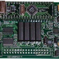
The A/D is a dual-channel, 12-bit, successive-approximation converter that was chosen
for its low cost and small size. The intention of this hardware design was more to show
off the capabilities of the MPSSE and less to provide a large-scale or highly accurate
data acquisition system. That said, 12 bits (1.2-millivolt resolution) is likely to be more
than enough for most voltage measurements on the 0-5 volt range.
Since the voltage reference for this converter is tied to the VDD line internally, VDD is
the reference and can be any value from 4.5-5.5 volts. Since this A/D is communicating
digitally with a 5-volt system, taking VDD below 4.5 volts could cause damage and
would definitely affect accuracy. In this design, the VDD line for the converter is brought
out to the interface header via J2, and either the 5-volt supply from the USB port can be
used or an external voltage provided through H1. For most applications, the 5-volt
power from the USB port should work just fine.
The DAC employed in this design is also a 12-bit, dual-channel device that has its
reference voltage pin brought out to interface Header H1. If Jumper J3 is set to
positions 1 and 2, the output voltage range will be from 0 to approximately 5 volts or
whatever the voltage is currently on the USB port. If Jumper J3 is set to positions 2 and
3, then an external reference can be used in the range of 0-5 volts. For example, if an
external voltage reference of 2 volts is used, then the output voltage range of the DAC
will be 0-2 volts with a resolution of 490 microvolts (2.0/4096).
The chip used to implement the 12-bit digital I/O bus (also referred to as an I/O
Expander) is a Microchip MCP23016, and it can have each of its I/O lines configured as
either input or output. Since the I/O Expander does not have a chip select line, an
external buffer (U3) was used to prevent the clock line from initiating a reply on the data
line while the MPSSE is communicating with another device.
The four relays used in this design are SPST reed relays, and they require very little
current (10mA) to energize their internal 5-volt coil--perfect for USB port-powered
applications. They do not need internal protection diodes since the ULN2003A already
has the protection diodes built in. When the MCP23016 first powers up, its I/O pins are
set to input, so 100K pull-down resistors were added to ensure the relays would all be
off.
FT2232C
The best source of information on the FT2232C is, of course, the datasheet. To briefly
summarize some of its high points, the two channels of the chip can be individually
configured to use either the Virtual COM Port drivers (these make the port look like an
RS232 serial port to the host application) or the DLL drivers. Each channel can be
configured for any of the various modes of operation (MPSSE is only available on
Channel A), and these selections are made via writing to an EEPROM device that is
connected to the FT2232C.
4
Related parts for DLP-2232DAQ
Image
Part Number
Description
Manufacturer
Datasheet
Request
R

Part Number:
Description:
MODULE USB-TO-TTL PARL FIFO CONV
Manufacturer:
DLP Design Inc
Datasheet:

Part Number:
Description:
KIT DEV DLP LIGHTCOMANDER
Manufacturer:
Logic
Datasheet:

Part Number:
Description:
MODULE DATA-ACQUISITION 8-CH
Manufacturer:
DLP Design Inc
Datasheet:

Part Number:
Description:
MODULE DATA-ACQUISITION 20-CH
Manufacturer:
DLP Design Inc
Datasheet:

Part Number:
Description:
RFID READER/WRITER SNGL-CH OEM
Manufacturer:
DLP Design Inc
Datasheet:

Part Number:
Description:
Interface Modules & Development Tools DLP-245PL PACKAGED w/CCS Compiler
Manufacturer:
DLP Design Inc

Part Number:
Description:
Interface Modules & Development Tools DLP-245PB-G BOARD + CCS Compiler
Manufacturer:
DLP Design Inc
Datasheet:

Part Number:
Description:
Interface Modules & Development Tools DLP-TILT SENSOR ACCEL VIBRATION
Manufacturer:
DLP Design Inc

Part Number:
Description:
MODULE USB-MCU FT245RL W/16F877A
Manufacturer:
DLP Design Inc
Datasheet:

Part Number:
Description:
MODULE USB-TO-FPGA TRAINING TOOL
Manufacturer:
DLP Design Inc
Datasheet:

Part Number:
Description:
MODULE USB-MCU FT232R W/18F2410
Manufacturer:
DLP Design Inc
Datasheet:

Part Number:
Description:
MODULE USB-MCU FT245RL W/SX48
Manufacturer:
DLP Design Inc
Datasheet:

Part Number:
Description:
MODULE USB-MCU FT2232D W/16F877A
Manufacturer:
DLP Design Inc
Datasheet:

Part Number:
Description:
MODULE USB-TO-FPGA SPARTAN3
Manufacturer:
DLP Design Inc
Datasheet:

Part Number:
Description:
MOD USB-MCU FT245RL W/18LF8722
Manufacturer:
DLP Design Inc
Datasheet: