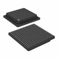
AD6635BB Analog Devices Inc, AD6635BB Datasheet - Page 30

AD6635BB
Manufacturer Part Number
AD6635BB
Description
IC,RF/Baseband Circuit,CMOS,BGA,324PIN,PLASTIC
Manufacturer
Analog Devices Inc
Series
AD6635r
Datasheet
1.AD6635BBPCB.pdf
(60 pages)
Specifications of AD6635BB
Rohs Status
RoHS non-compliant
Rf Type
Cellular, CDMA2000, EDGE, GPRS, GSM
Number Of Mixers
1
Current - Supply
880mA
Voltage - Supply
3 V ~ 3.6 V
Package / Case
324-BGA
Frequency
-
Gain
-
Noise Figure
-
Secondary Attributes
-
Lead Free Status / RoHS Status
Available stocks
Company
Part Number
Manufacturer
Quantity
Price
Part Number:
AD6635BB
Manufacturer:
ADI/亚德诺
Quantity:
20 000
AD6635
M
10
11
12
13
14
15
16
17
18
19
20
21
22
23
24
25
26
27
28
29
30
31
32
RAM COEFFICIENT FILTER
The final signal processing stage for each individual channel is a
sum-of-products decimating filter with programmable coeffi-
cients. A simplified block diagram is shown below. The data
memories I-RAM and Q-RAM store the 160 most recent com-
plex samples from the previous filter stage with 20-bit resolution.
The coefficient memory, CMEM, stores up to 256 coefficients
with 20-bit resolution. On every CLK cycle, one tap for I and
one tap for Q are calculated using the same coefficients. The
RCF output consists of 24-bit data.
2
3
4
5
6
7
8
9
CIC5
Figure 30. RAM Coefficient Filter (RCF) Block Diagram
Table IV. SSB CIC5 Alias Rejection Table (f
Bandwidths are given as percentage of f
–50 dB –60 dB –70 dB –80 dB –90 dB –100 dB
10.227 8.078
7.924 6.367
6.213 5.022
5.068 4.107
4.267 3.463
3.680 2.989
3.233 2.627
2.881 2.342
2.598 2.113
2.365 1.924
2.170 1.765
2.005 1.631
1.863 1.516
1.740 1.416
1.632 1.328
1.536 1.250
1.451 1.181
1.375 1.119
1.307 1.064
1.245 1.013
1.188 0.967
1.137 0.925
1.090 0.887
1.046 0.852
1.006 0.819
0.969 0.789
0.934 0.761
0.902 0.734
0.872 0.710
0.844 0.687
0.818 0.666
QIN
IIN
160
256
160
C-RAM
Q-RAM
I-RAM
20B
20B
20B
6.393
5.110
4.057
3.326
2.808
2.425
2.133
1.902
1.716
1.563
1.435
1.326
1.232
1.151
1.079
1.016
0.960
0.910
0.865
0.824
0.786
0.752
0.721
0.692
0.666
0.641
0.618
0.597
0.577
0.559
0.541
5.066
4.107
3.271
2.687
2.270
1.962
1.726
1.540
1.390
1.266
1.162
1.074
0.998
0.932
0.874
0.823
0.778
0.737
0.701
0.667
0.637
0.610
0.584
0.561
0.540
0.520
0.501
0.484
0.468
0.453
0.439
QOUT
IOUT
SAMP2
4.008
1.125
1.025
0.941
0.870
0.809
0.755
0.708
0.667
0.630
0.597
0.568
0.541
0.516
0.494
0.474
0.455
0.437
0.421
0.406
0.392
0.379
0.367
0.355
3.297
2.636
2.170
1.836
1.588
1.397
1.247
SAMP2
.
3.183
2.642
2.121
1.748
1.480
1.281
1.128
1.007
0.909
0.828
0.760
0.703
0.653
0.610
0.572
0.539
0.509
0.483
0.459
0.437
0.417
0.399
0.383
0.367
0.353
0.340
0.328
0.317
0.306
0.297
0.287
= 1).
–30–
RCF Decimation Register
Each RCF channel can be used to decimate the data rate. The
decimation register is an 8-bit register and can decimate from
1 to 256. The RCF decimation is stored in 0xA0 in the form of
MRCF – 1. The input rate to the RCF is f
RCF Decimation Phase
The RCF decimation phase can be used to synchronize multiple
filters within a chip. This is useful when using multiple channels
within the AD6635 to implement a polyphase filter allowing the
resources of several RCF filters to be paralleled. In such an
application, two RCF filters would be processing the same data
from the CIC5. However, each filter will be delayed by one half
the decimation rate, thus creating a 180∞ phase difference between
the two halves.
The AD6635 filter channel uses the value stored in this register
to preload the RCF counter. Therefore, instead of starting from
0 (coefficient number 0), the counter is loaded with
thus creating an offset in the processing that should be equiva-
lent to the required processing delay. The number of channels
or RCFs used to process one carrier is used in the above equa-
tion. f
input sample rate to the RCF from the CIC5 stage. This data is
stored in 0xA1 as an 8-bit number. The RCF decimation phase
can be used only when the ratio of RCF decimation and num-
ber of RCFs used is an integer.
RCF Filter Length
The maximum number of taps this filter can calculate, N
given by the equation below. The value N
the Channel register within the AD6635 at address 0xA2.
The function “min” used above gives the minimum of all the
expressions inside the parenthesis.
The RCF coefficients are located in addresses 0x00 to 0x7F and
are interpreted as 20-bit twos complement numbers. When
writing the coefficient RAM, the lower addresses will be multi-
plied by relatively older data from the CIC5 and the higher
coefficient addresses will be multiplied by relatively newer data
from the CIC5. The coefficients need not be symmetric and the
coefficient length, N
are symmetric, then both sides of the impulse response must be
written into the coefficient RAM.
Although the base memory for coefficients is only 128 words
long, the actual length is 256 words long. There are two pages,
each 128 words long. The page is selected by Bit 8 of 0xA4.
Counter
CLK
=
is the input clock rate to the AD6635 and f
decimation phase Number of channels used
N
TAPS
RCF decimationineach channel
TAPS
£
min
, may be even or odd. If the coefficients
Ê
Á
Ë
¥
f
CLK
f
SAMP
¥
M
5
RCF
TAPS
SAMP5
,
160
– 1 is written to
.
ˆ
˜
¯
¥
RCF
f
RCF
REV. 0
is the
TAPS
¥
f
CLK
, is


