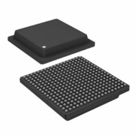
AD6635BB Analog Devices Inc, AD6635BB Datasheet - Page 58

AD6635BB
Manufacturer Part Number
AD6635BB
Description
IC,RF/Baseband Circuit,CMOS,BGA,324PIN,PLASTIC
Manufacturer
Analog Devices Inc
Series
AD6635r
Datasheet
1.AD6635BBPCB.pdf
(60 pages)
Specifications of AD6635BB
Rohs Status
RoHS non-compliant
Rf Type
Cellular, CDMA2000, EDGE, GPRS, GSM
Number Of Mixers
1
Current - Supply
880mA
Voltage - Supply
3 V ~ 3.6 V
Package / Case
324-BGA
Frequency
-
Gain
-
Noise Figure
-
Secondary Attributes
-
Lead Free Status / RoHS Status
Available stocks
Company
Part Number
Manufacturer
Quantity
Price
Part Number:
AD6635BB
Manufacturer:
ADI/亚德诺
Quantity:
20 000
AD6635
INTERNAL WRITE ACCESS
Up to 20 bits of data (as needed) can be written by the process
described below. Any high order bytes that are needed are writ-
ten to the corresponding data registers defined in the external
3-bit address space. The least significant byte is then written to
DR0 at address (000). When a write to DR0 is detected, the
internal microprocessor port state machine then moves the data
in DR2–DR0 to the internal address pointed to by the address
in the LAR and AMR.
Write Pseudocode
void write_micro(ext_address, int data);
main();
{
/* This code shows the programming of the NCO
phase offset register using the write_micro
function as defined above. The variable address
is the External Address A[2:0]
value to be placed in the external interface
register.
Internal Address = 0x87
// holding registers for NCO phase byte wide
access data
int d1, d0;
// NCO phase word
NCO_PHASE = 0xCBEF;
// write ACR
write_micro(7, 0x03 );
// write CAR
write_micro(6, 0x87);
// write DR1 with D[15:8]
d1 = (NCO_PHASE & 0xFF00) >> 8;
write_micro(1, d1);
// write DR0 with D[7:0]
// On this write all data is transferred to the
internal address
d0 = NCO_PHASE & 0xFF;
write_micro(0, d0);
}
// end of main
(16-bits wide)
*/
and data is the
–58–
INTERNAL READ ACCESS
A read is performed by first writing the CAR and AMR, as with
a write. The data registers (DR2–DR0) are then read in the
reverse order that they were written. First, the least significant
byte of the data (D[7:0]) is read from DR0. On this transac-
tion, the high bytes of the data are moved from the internal
address pointed to by the CAR and AMR into the remaining
data registers (DR2–DR1). This data can then be read from the
data registers using the appropriate 3-bit addresses. The num-
ber of data registers used depends solely on the amount of data
to be read or written. Any unused bit in a data register should
be masked out for a read.
Read Pseudocode
int read_micro(ext_address);
main();
{
/* This code shows the reading of
RCF coefficient using the read_micro function
as defined above. The variable address is the
External Address A[2..0].
Internal Address = 0x000
// holding registers for the coefficient
int d2, d1, d0;
// coefficient
long coefficient;
// write AMR
write_micro(7, 0x00 );
// write LAR
write_micro(6, 0x00);
/* read D[7:0] from DR0,
from the Internal Registers to the interface
registers on this access
d0 = read_micro(0) & 0xFF;
// read D[15:8] from DR1
d1 = read_micro(1) & 0xFF;
// read D[23:16] from DR2
d2 = read_micro(2) & 0x0F;
coefficient = d0 + (d1 << 8) + (d2 << 16);
}
*/
// end of main
(20-bits wide)
All data is moved
*/
the first
REV. 0


