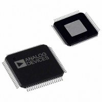
AD9726BSVZRL Analog Devices Inc, AD9726BSVZRL Datasheet - Page 23

AD9726BSVZRL
Manufacturer Part Number
AD9726BSVZRL
Description
IC,D/A CONVERTER,SINGLE,16-BIT,CMOS,TQFP,80PIN
Manufacturer
Analog Devices Inc
Series
TxDAC+®r
Datasheet
1.AD9726BSVZRL.pdf
(24 pages)
Specifications of AD9726BSVZRL
Number Of Bits
16
Data Interface
Parallel
Number Of Converters
1
Voltage Supply Source
Analog and Digital
Power Dissipation (max)
575mW
Operating Temperature
-40°C ~ 85°C
Mounting Type
Surface Mount
Package / Case
80-TQFP Exposed Pad, 80-eTQFP, 80-HTQFP, 80-VQFP
Lead Free Status / RoHS Status
Lead free / RoHS Compliant
For Use With
AD9726-EBZ - BOARD EVAL FOR AD9726
Settling Time
-
Lead Free Status / RoHS Status
Lead free / RoHS Compliant
Available stocks
Company
Part Number
Manufacturer
Quantity
Price
Company:
Part Number:
AD9726BSVZRL
Manufacturer:
Analog Devices Inc
Quantity:
10 000
sync logic should be resynchronized by asserting SYNCUPD
at the next convenient time.
In manual mode, users can choose when to update the sync
logic. When operating with burst data, issuing a sync update
between active bursts updates the system without risking the
loss of any data. In fact, because SYNCUPD always forces a
resynchronization regardless of operational mode, even users in
fully automatic mode can reduce the possibility of data loss by
occasionally forcing a sync update during idle activity.
If either the data clock or the DAC clock is interrupted for any
reason, a SYNCUPD should always be executed to ensure that
data bus and DAC clock phase alignment remains optimized.
SYNC External Mode
Going beyond manual mode, sync external mode offers a
greater level of control and can be useful if multiple DAC
channels are employed in an application. Enable sync external
mode by asserting the SYNCEXT bit (Bit 5) in SPI Register
0x16. Manual mode must also be enabled.
Rev. B | Page 23 of 24
The four channels into which each incoming data-word is
multiplexed are called quadrants. In any mode, the current
quadrant value can always be read back via SYNCOUT (Bits
[1:0] of SPI Register 0x15). At sync update, the logic chooses the
optimal quadrant and refreshes the value of SYNCOUT.
It is also possible to enter a value into SYNCIN (Bits [4:3] of SPI
Register 0x16). When external mode is enabled, the logic oper-
ates as expected, except that the quadrant value in SYNCIN is
used following an update. This can be used to align delays
between multiple device outputs.
Operating With SPI Disabled
If the SPI_DIS pin is connected high to ADVDD and the SPI is
disabled, the sync logic is placed into manual mode.
SYNCALRM status can then be monitored in hardware via the
unused SPI pin SDO (54), and SYNCUPD requests can be
entered in hardware via the unused SPI pin SCLK (56). If these
two pins are connected together, fully automatic sync operation
can be achieved.
AD9726


