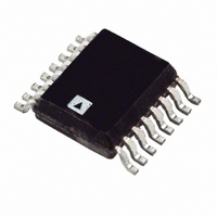
ADCMP561BRQZ Analog Devices Inc, ADCMP561BRQZ Datasheet - Page 10

ADCMP561BRQZ
Manufacturer Part Number
ADCMP561BRQZ
Description
Dual High Speed PECL Comparator
Manufacturer
Analog Devices Inc
Type
with Latchr
Datasheet
1.ADCMP562BRQZ.pdf
(16 pages)
Specifications of ADCMP561BRQZ
Number Of Elements
2
Output Type
Complementary, Differential, Open-Emitter, PECL
Voltage - Supply
±4.75 V ~ 5.25 V
Mounting Type
Surface Mount
Package / Case
16-LSSOP (0.154", 3.91mm Width)
Number Of Elements
2
Input Offset Voltage
10mV
Input Bias Current (typ)
10uA
Response Time
700ns
Single Supply Voltage (typ)
Not RequiredV
Dual Supply Voltage (typ)
-5.2/5V
Supply Current (max)
13/28@±5VmA
Power Supply Requirement
Dual
Common Mode Rejection Ratio
80dB
Voltage Gain In Db
63dB
Power Supply Rejection Ratio
85dB
Single Supply Voltage (min)
Not RequiredV
Single Supply Voltage (max)
Not RequiredV
Dual Supply Voltage (min)
-4.96/4.75V
Dual Supply Voltage (max)
-5.45/5.25V
Power Dissipation
250mW
Operating Temp Range
-40C to 85C
Operating Temperature Classification
Industrial
Mounting
Surface Mount
Pin Count
16
Package Type
QSOP
No. Of Comparators
2
Ic Output Type
Differential
Output Compatibility
PECL
Supply Current
3.2mA
Supply Voltage Range
4.75V To 5.25V
Amplifier Case Style
QSOP
No. Of Pins
16
Lead Free Status / RoHS Status
Lead free / RoHS Compliant
For Use With
EVAL-ADCMP561BRQZ - BOARD EVALUATION ADCMP561BRQZ
Lead Free Status / Rohs Status
Compliant
Available stocks
Company
Part Number
Manufacturer
Quantity
Price
Part Number:
ADCMP561BRQZ
Manufacturer:
AD
Quantity:
20 000
ADCMP561/ADCMP562
TIMING INFORMATION
Figure 18 shows the compare and latch features of the ADCMP561/ADCMP562. Table 4 describes the terms in the diagram.
Table 4. Timing Descriptions
Symbol
t
t
t
t
t
t
t
t
t
V
PDH
PDL
PLOH
PLOL
H
PL
S
R
F
OD
Timing
Input to Output High Delay
Input to Output Low Delay
Latch Enable to Output High Delay
Latch Enable to Output Low Delay
Minimum Hold Time
Minimum Latch Enable Pulse Width
Minimum Setup Time
Output Rise Time
Output Fall Time
Voltage Overdrive
INPUT VOLTAGE
LATCH ENABLE
LATCH ENABLE
DIFFERENTIAL
Q OUTPUT
Q OUTPUT
V
IN
Description
Propagation delay measured from the time the input signal crosses the reference (± the
input offset voltage) to the 50% point of an output low-to-high transition.
Propagation delay measured from the time the input signal crosses the reference (± the
input offset voltage) to the 50% point of an output high-to-low transition.
Propagation delay measured from the 50% point of the latch enable signal low-to-high
transition to the 50% point of an output low-to-high transition.
Propagation delay measured from the 50% point of the latch enable signal low-to-high
transition to the 50% point of an output high-to-low transition.
Minimum time after the negative transition of the latch enable signal that the input signal
must remain unchanged to be acquired and held at the outputs.
Minimum time the latch enable signal must be high to acquire an input signal change.
Minimum time before the negative transition of the latch enable signal that an input
signal change must be present to be acquired and held at the outputs.
Amount of time required to transition from a low to a high output as measured at the
20% and 80% points.
Amount of time required to transition from a high to a low output as measured at the
20% and 80% points.
Difference between the differential input and reference input voltages.
V
Figure 18. System Timing Diagram
t
S
OD
t
t
PDL
PDH
Rev. A | Page 10 of 16
t
H
t
R
t
F
t
PL
t
t
PLOH
PLOL
50%
V
50%
50%
REF
± V
OS


