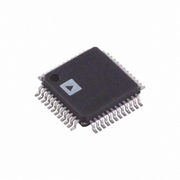
ADUC7032BSTZ-8L-RL Analog Devices Inc, ADUC7032BSTZ-8L-RL Datasheet - Page 45

ADUC7032BSTZ-8L-RL
Manufacturer Part Number
ADUC7032BSTZ-8L-RL
Description
IC,Battery Management,QFP,48PIN,PLASTIC
Manufacturer
Analog Devices Inc
Series
MicroConverter® ADuC7xxxr
Datasheet
1.EVAL-ADUC7032QSPZ.pdf
(116 pages)
Specifications of ADUC7032BSTZ-8L-RL
Core Processor
ARM7
Core Size
16/32-Bit
Speed
20.48MHz
Connectivity
LIN, SPI, UART/USART
Peripherals
POR, PSM, Temp Sensor, WDT
Number Of I /o
9
Program Memory Size
96KB (96K x 8)
Program Memory Type
FLASH
Ram Size
6K x 8
Voltage - Supply (vcc/vdd)
3.5 V ~ 18 V
Data Converters
A/D 2x16b
Oscillator Type
Internal
Operating Temperature
-40°C ~ 105°C
Package / Case
48-LQFP
Lead Free Status / RoHS Status
Lead free / RoHS Compliant
Eeprom Size
-
Lead Free Status / Rohs Status
Compliant
Bit
15
14 to 13
12 to 10
9
8
7 to 6
5 to 4
3 to 0
Current Channel ADC Control Register
Name: ADC0CON
Address: 0xFFFF050C
Default Value: 0x00002
Access: Read/write
Function: The current channel ADC control MMR is a 16-bit register that is used to configure the I-ADC. Note that if the current ADC
is reconfigured via ADC0CON, the voltage and temperature ADCs are also reset.
Table 37. ADC0CON MMR Bit Designations
Description
Current Channel ADC Enable.
Current Source Enable.
Not Used. Reserved for future functionality and should be written as 0.
Current Channel ADC Output Coding.
Not Used. Reserved for future functionality and should be written as 0.
Current Channel ADC Input Select.
Current Channel ADC Reference Select.
Current Channel ADC Gain Select. (Note that nominal I-ADC full-scale input voltage = VREF/GAIN.)
Set to 1 by user code to enable the I-ADC.
Cleared to 0 to power down the I-ADC and reset the respective ADC ready bit in the ADCSTA MMR to 0.
00 = current sources off.
01 = enable 50 μA current source on IIN+.
10 = enable 50 μA current source on IIN−.
11 = enable 50 μA current source on both IIN− and IIN+.
Set to 1 by user code to configure I-ADC output coding as unipolar.
Cleared to 0 by user code to configure I-ADC output coding as twos complement.
00 = internal, 1.2 V precision reference selected. In ADC low power mode, the voltage reference selection is controlled by
ADCMDE[5].
01 = external reference inputs (VREF, GND_SW) selected.
10 = external reference inputs divided by 2 ((VREF, GND_SW)/2) selected allows an external reference up to REG_AVDD.
11 = (REG_AVDD, AGND)/2 selected.
0000 = I-ADC gain = 1.
0001 = I-ADC gain = 2.
0010 = I-ADC gain = 4.
0011 = I-ADC gain = 8.
0100 = I-ADC gain = 16.
0101 = I-ADC gain = 32.
0110 = I-ADC gain = 64.
0111 = I-ADC gain = 128.
1000 = I-ADC gain = 256.
1001 = I-ADC gain = 512.
1xxx = I-ADC gain is undefined.
00 = IIN+, IIN−.
01 = IIN−, IIN−. Diagnostic, internal short configuration.
10 = ADC reference/136, 0 V. Diagnostic, test voltage for gain settings ≤ 128.
11 = not defined.
Rev.0 | Page 45 of 116
ADuC7032-8L


