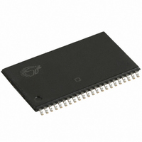
CY7C1020CV33-15ZSXE Cypress Semiconductor Corp, CY7C1020CV33-15ZSXE Datasheet - Page 6

CY7C1020CV33-15ZSXE
Manufacturer Part Number
CY7C1020CV33-15ZSXE
Description
IC,SRAM,32KX16,CMOS,TSOP,44PIN,PLASTIC
Manufacturer
Cypress Semiconductor Corp
Datasheet
1.CY7C1020CV33-15ZSXE.pdf
(13 pages)
Specifications of CY7C1020CV33-15ZSXE
Format - Memory
RAM
Memory Type
SRAM - Asynchronous
Memory Size
512K (32K x 16)
Speed
15ns
Interface
Parallel
Voltage - Supply
3 V ~ 3.6 V
Operating Temperature
-40°C ~ 125°C
Package / Case
44-TSOP II
Density
512Kb
Access Time (max)
15ns
Sync/async
Asynchronous
Architecture
Not Required
Clock Freq (max)
Not RequiredMHz
Operating Supply Voltage (typ)
3.3V
Address Bus
15b
Package Type
TSOP-II
Operating Temp Range
-40C to 125C
Number Of Ports
1
Supply Current
85mA
Operating Supply Voltage (min)
2.97V
Operating Supply Voltage (max)
3.63V
Operating Temperature Classification
Automotive
Mounting
Surface Mount
Pin Count
44
Word Size
16b
Number Of Words
32K
Lead Free Status / RoHS Status
Lead free / RoHS Compliant
Lead Free Status / RoHS Status
Lead free / RoHS Compliant
AC Test Loads and Waveforms
Switching Characteristics
Over the Operating Range
Document Number: 38-05133 Rev. *H
Read Cycle
t
t
t
t
t
t
t
t
t
t
t
t
t
t
Write Cycle
t
t
t
t
t
t
t
t
t
t
t
Notes
OUTPUT
RC
AA
OHA
ACE
DOE
LZOE
HZOE
LZCE
HZCE
PU
PD
DBE
LZBE
HZBE
WC
SCE
AW
HA
SA
PWE
SD
HD
LZWE
HZWE
BW
4. Test conditions assume signal transition time of 3 ns or less, timing reference levels of 1.5 V, input pulse levels of 0 to 3.0 V.
5. At any given temperature and voltage condition, t
6. t
7. This parameter is guaranteed by design and is not tested.
8. The internal Write time of the memory is defined by the overlap of CE LOW, WE LOW and BHE/BLE LOW. CE, WE and BHE/BLE must be LOW to initiate a Write, and
Parameter
[7]
[7]
the transition of these signals can terminate the Write. The input data set-up and hold timing should be referenced to the leading edge of the signal that terminates the Write.
HZOE
3.3 V
, t
HZBE
30 pF
[8]
, t
HZCE
Read cycle time
Address to data valid
Data hold from address change
CE LOW to data valid
OE LOW to data valid
OE LOW to low Z
OE HIGH to high Z
CE LOW to low Z
CE HIGH to high Z
CE LOW to power-up
CE HIGH to power-down
Byte enable to data valid
Byte enable to low Z
Byte disable to high Z
Write cycle time
CE LOW to write end
Address set-up to write end
Address hold from write end
Address set-up to write start
WE pulse width
Data set-up to write end
Data hold from write end
WE HIGH to low Z
WE LOW to high Z
Byte enable to end of write
, and t
R 317
(a)
HZWE
[4]
are specified with a load capacitance of 5 pF as in part (c) of AC Test Loads. Transition is measured 500 mV from steady-state voltage.
351
R2
Description
[5]
[5]
[5]
[5, 6]
[5, 6]
GND
[5, 6]
3.0 V
Rise Time: 1 V/ns
HZCE
[4]
is less than t
10%
LZCE
90%
ALL INPUT PULSES
, t
HZOE
Min
10
10
–
3
–
–
0
–
3
–
0
–
–
0
–
8
7
0
0
7
5
0
3
–
7
is less than t
(b)
–10
Max
LZOE
10
10
10
–
–
5
–
5
–
5
–
5
–
5
–
–
–
–
–
–
–
–
–
5
–
, and t
Fall Time: 1 V/ns
90%
HZWE
10%
Min
12
12
–
3
–
–
0
–
3
–
0
–
–
0
–
9
8
0
0
8
6
0
3
–
8
is less than t
–12
Max
12
12
12
OUTPUT
LZWE
–
–
6
–
6
–
6
–
6
–
6
–
–
–
–
–
–
–
–
–
6
–
High Z characteristics:
for any given device.
3.3 V
Min
(c)
15
15
10
10
10
–
3
–
–
0
–
3
–
0
–
–
0
–
0
0
8
0
3
–
9
CY7C1020CV33
5 pF
–15
R 317
Max
15
15
15
–
–
7
–
7
–
7
–
7
–
7
–
–
–
–
–
–
–
–
–
7
–
Page 6 of 13
Unit
351
ns
ns
ns
ns
ns
ns
ns
ns
ns
ns
ns
ns
ns
ns
ns
ns
ns
ns
ns
ns
ns
ns
ns
ns
ns
R2
[+] Feedback


