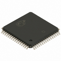
CY7C4265-10ASXC Cypress Semiconductor Corp, CY7C4265-10ASXC Datasheet - Page 16

CY7C4265-10ASXC
Manufacturer Part Number
CY7C4265-10ASXC
Description
IC,FIFO,16KX18,SYNCHRONOUS,CMOS,QFP,64PIN,PLASTIC
Manufacturer
Cypress Semiconductor Corp
Series
CY7Cr
Datasheet
1.CY7C4265-15AXC.pdf
(25 pages)
Specifications of CY7C4265-10ASXC
Function
Synchronous
Memory Size
288K (16K x 18)
Data Rate
100MHz
Access Time
8ns
Voltage - Supply
3.3V
Operating Temperature
-40°C ~ 85°C
Mounting Type
Surface Mount
Package / Case
64-LQFP
Lead Free Status / RoHS Status
Lead free / RoHS Compliant
Available stocks
Company
Part Number
Manufacturer
Quantity
Price
Company:
Part Number:
CY7C4265-10ASXC
Manufacturer:
Cypress Semiconductor Corp
Quantity:
10 000
Architecture
The CY7C4256/65 consists of an array of 8K/16K words of 18
bits each (implemented by a dual-port array of SRAM cells), a
read pointer, a write pointer, control signals (RCLK, WCLK, REN,
WEN, RS), and flags (EF, PAE, HF, PAF, FF). The CY7C4265
also includes the control signals WXI, RXI, WXO, RXO for depth
expansion.
Resetting the FIFO
Upon power up, the FIFO must be reset with a Reset (RS) cycle.
This causes the FIFO to enter the Empty condition signified by
EF being LOW. All data outputs go LOW after the falling edge of
RS only if OE is asserted. For the FIFO to reset to its default
state, a falling edge must occur on RS and the user must not read
or write while RS is LOW.
FIFO Operation
When the WEN signal is active (LOW), data present on the D
pins is written into the FIFO on each rising edge of the WCLK
signal. Similarly, when the REN signal is active LOW, data in the
FIFO memory are presented on the Q
presented on each rising edge of RCLK while REN is active LOW
and OE is LOW. REN must set up t
a valid read function. WEN must occur tENS before WCLK for it
to be a valid write function.
An output enable (OE) pin is provided to three-state the Q
outputs when OE is deasserted. When OE is enabled (LOW),
data in the output register is available to the Q
t
on the FIFO that is read enabled.
The FIFO contains overflow circuitry to disallow additional writes
when the FIFO is full, and under flow circuitry to disallow
additional reads when the FIFO is empty. An empty FIFO
maintains the data of the last valid read on its Q
after additional reads occur.
Programming
The CY7C4265 devices contain two 14-bit offset registers. Data
present on D
from Empty (Full) that the Almost Empty (Almost Full) flags
become active. If the user elects not to program the FIFO’s flags,
the default offset values are used (see
LD pin is set LOW and WEN is set LOW, data on the inputs D
is written into the Empty offset register on the first LOW-to-HIGH
transition of the Write Clock (WCLK). When the LD pin and WEN
are held LOW then data is written into the Full offset register on
the second LOW-to-HIGH transition of the Write Clock (WCLK).
The third transition of the Write Clock (WCLK) again writes to the
Empty offset register (see
does not have to occur at one time. One or two offset registers
can be written and then, by bringing the LD pin HIGH, the FIFO
is returned to normal read/write operation. When the LD pin is
Document #: 38-06004 Rev. *G
OE
Note
37. The same selection sequence applies to reading from the registers. REN is enabled and read is performed on the LOW-to-HIGH transition of RCLK.
. If devices are cascaded, the OE function only outputs data
0–13
during a program write determines the distance
Table
4). Writing all offset registers
ENS
0–17
Table
before RCLK for it to be
outputs. New data is
4). When the Load
0–17
0–17
outputs after
outputs even
0–17
0–17
0–13
set LOW, and WEN is LOW, the next offset register in sequence
is written.
The contents of the offset registers can be read on the output
lines when the LD pin is set LOW and REN is set LOW; then,
data can be read on the LOW-to-HIGH transition of the Read
Clock (RCLK).
Table 4. Write Offset Register
Flag Operation
The CY7C4265 devices provide five flag pins to indicate the
condition of the FIFO contents. Empty and Full are synchronous.
PAE and PAF are synchronous if V
Full Flag
The Full Flag (FF) goes LOW when device is Full. Write opera-
tions are inhibited whenever FF is LOW regardless of the state
of WEN. FF is synchronized to WCLK: it is exclusively updated
by each rising edge of WCLK.
Empty Flag
The Empty Flag (EF) goes LOW when the device is empty. Read
operations are inhibited whenever EF is LOW, regardless of the
state of REN. EF is synchronized to RCLK, i.e., it is exclusively
updated by each rising edge of RCLK.
Programmable Almost Empty/Almost Full Flag
The CY7C4265 features programmable Almost Empty and
Almost Full Flags. Each flag can be programmed (described in
the Programming section) a specific distance from the corre-
sponding boundary flags (Empty or Full). When the FIFO
contains the number of words or fewer for which the flags have
been programmed, the PAF or PAE are asserted, signifying that
the FIFO is either Almost Full or Almost Empty. See
page 17 for a description of programmable flags.
When the SMODE pin is tied LOW, the PAF flag signal transition
is caused by the rising edge of the write clock and the PAE flag
transition is caused by the rising edge of the read clock.
LD
0
0
1
1
WEN
0
1
0
1
WCLK
[37]
Writing to offset registers:
Empty Offset
Full Offset
No Operation
Write Into FIFO
No Operation
CC
/SMODE is tied to V
Selection
CY7C4265
Page 16 of 25
Table 5
SS
.
on
[+] Feedback


