SI1902DL-T1-E3 Vishay, SI1902DL-T1-E3 Datasheet - Page 6
SI1902DL-T1-E3
Manufacturer Part Number
SI1902DL-T1-E3
Description
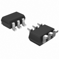
MOSFET N-CH DUAL 20V SC70-6
Manufacturer
Vishay
Series
TrenchFET®r
Type
Power MOSFETr
Specifications of SI1902DL-T1-E3
Transistor Polarity
N-Channel
Fet Type
2 N-Channel (Dual)
Fet Feature
Logic Level Gate
Rds On (max) @ Id, Vgs
385 mOhm @ 660ma, 4.5V
Drain To Source Voltage (vdss)
20V
Current - Continuous Drain (id) @ 25° C
660mA
Vgs(th) (max) @ Id
1.5V @ 250µA
Gate Charge (qg) @ Vgs
1.2nC @ 4.5V
Power - Max
270mW
Mounting Type
Surface Mount
Package / Case
SC-70-6, SC-88, SOT-363
Minimum Operating Temperature
- 55 C
Configuration
Dual
Resistance Drain-source Rds (on)
0.385 Ohm @ 4.5 V
Drain-source Breakdown Voltage
20 V
Gate-source Breakdown Voltage
+/- 12 V
Continuous Drain Current
0.66 A
Power Dissipation
270 mW
Maximum Operating Temperature
+ 150 C
Mounting Style
SMD/SMT
Continuous Drain Current Id
660mA
Drain Source Voltage Vds
20V
On Resistance Rds(on)
2ohm
Rds(on) Test Voltage Vgs
4.5V
Threshold Voltage Vgs Typ
1.5V
Rohs Compliant
Yes
Number Of Elements
2
Polarity
N
Channel Mode
Enhancement
Drain-source On-res
0.385Ohm
Drain-source On-volt
20V
Gate-source Voltage (max)
±12V
Operating Temp Range
-55C to 150C
Operating Temperature Classification
Military
Mounting
Surface Mount
Pin Count
6
Package Type
SC-70
Module Configuration
Dual
Lead Free Status / RoHS Status
Lead free / RoHS Compliant
Lead Free Status / RoHS Status
Lead free / RoHS Compliant, Lead free / RoHS Compliant
Other names
SI1902DL-T1-E3TR
Available stocks
Company
Part Number
Manufacturer
Quantity
Price
Company:

Part Number:
SI1902DL-T1-E3
Manufacturer:
Vishay/Siliconix
Quantity:
62 955
Part Number:
SI1902DL-T1-E3
Manufacturer:
VISHAY/威世
Quantity:
20 000


INTRODUCTION
This technical note discusses the pin-outs, package outlines,
pad patterns, evaluation board layout, and thermal
performance
MOSFETs in the SC-70 package. These new Vishay Siliconix
devices are intended for small-signal applications where a
miniaturized package is needed and low levels of current
(around 250 mA) need to be switched, either directly or by
using a level shift configuration. Vishay provides these devices
with a range of on-resistance specifications in 6-pin versions.
The
on-resistance values and enhanced thermal performance.
PIN-OUT
Figure 1 shows the pin-out description and Pin 1 identification
for the dual-channel SC-70 device in the 6-pin configuration.
For package dimensions see outline drawing SC-70 (6-Leads)
(http://www.vishay.com/doc?71154)
BASIC PAD PATTERNS
See Application Note 826, Recommended Minimum Pad
Patterns With Outline Drawing Access for Vishay Siliconix
MOSFETs, (http://www.vishay.com/doc?72286) for the 6-pin
SC-70. This basic pad pattern is sufficient for the low-power
Document Number: 71237
12-Dec-03
new
Recommended Pad Pattern and Thermal Performance
6-pin
Dual-Channel LITTLE FOOTR SC-70 6-Pin MOSFET
for
G
D
S
1
1
2
dual-channel
SC-70
1
2
3
SC-70 (6-LEADS)
SOT-363
FIGURE 1.
Top View
package
LITTLE
6
5
4
enables
D
G
S
2
1
2
FOOT
improved
power
applications for which this package is intended. For the 6-pin
device, increasing the pad patterns yields a reduction in
thermal resistance on the order of 20% when using a 1-inch
square with full copper on both sides of the printed circuit board
(PCB).
EVALUATION BOARDS FOR THE DUAL
SC70-6
The 6-pin SC-70 evaluation board (EVB) measures 0.6 inches
by 0.5 inches. The copper pad traces are the same as
described in the previous section, Basic Pad Patterns. The
board allows interrogation from the outer pins to 6-pin DIP
connections permitting test sockets to be used in evaluation
testing.
The thermal performance of the dual SC-70 has been
measured on the EVB with the results shown below. The
minimum recommended footprint on the evaluation board was
compared with the industry standard 1-inch square FR4 PCB
with copper on both sides of the board.
THERMAL PERFORMANCE
Junction-to-Foot Thermal Resistance
(the Package Performance)
Thermal performance for the dual SC-70 6-pin package
measured as junction-to-foot thermal resistance is 300_C/W
typical, 350_C/W maximum. The “foot” is the drain lead of the
device as it connects with the body. Note that these numbers
are somewhat higher than other LITTLE FOOT devices due to
the limited thermal performance of the Alloy 42 lead-frame
compared with a standard copper lead-frame.
Junction-to-Ambient Thermal Resistance
(dependent on PCB size)
The typical Rθ
state. Maximum ratings are 460_C/W for the dual. All figures
based on the 1-inch square FR4 test board. The following
example shows how the thermal resistance impacts power
dissipation for the dual 6-pin SC-70 package at two different
ambient temperatures.
JA
for the dual 6-pin SC-70 is 400_C/W steady
Vishay Siliconix
www.vishay.com
AN814
1
Related parts for SI1902DL-T1-E3
Image
Part Number
Description
Manufacturer
Datasheet
Request
R

Part Number:
Description:
Dual N-Channel 20-V (D-S) MOSFET
Manufacturer:
Vishay Siliconix
Datasheet:
Part Number:
Description:
Dual N-Channel 20-V (D-S) MOSFET
Manufacturer:
VISHAY [Vishay Siliconix]
Datasheet:


Part Number:
Description:
357-036-542-201 CARDEDGE 36POS DL .156 BLK LOPRO
Manufacturer:
Vishay
Datasheet:
Part Number:
Description:
357-036-542-201 CARDEDGE 36POS DL .156 BLK LOPRO
Manufacturer:
Vishay
Datasheet:
Part Number:
Description:
357-036-542-201 CARDEDGE 36POS DL .156 BLK LOPRO
Manufacturer:
Vishay
Datasheet:
Part Number:
Description:
357-036-542-201 CARDEDGE 36POS DL .156 BLK LOPRO
Manufacturer:
Vishay
Datasheet:
Part Number:
Description:
357-036-542-201 CARDEDGE 36POS DL .156 BLK LOPRO
Manufacturer:
Vishay
Datasheet:
Part Number:
Description:
357-036-542-201 CARDEDGE 36POS DL .156 BLK LOPRO
Manufacturer:
Vishay
Datasheet:
Part Number:
Description:
357-036-542-201 CARDEDGE 36POS DL .156 BLK LOPRO
Manufacturer:
Vishay
Datasheet:
Part Number:
Description:
357-036-542-201 CARDEDGE 36POS DL .156 BLK LOPRO
Manufacturer:
Vishay
Datasheet:
Part Number:
Description:
357-036-542-201 CARDEDGE 36POS DL .156 BLK LOPRO
Manufacturer:
Vishay
Datasheet:
Part Number:
Description:
357-036-542-201 CARDEDGE 36POS DL .156 BLK LOPRO
Manufacturer:
Vishay
Datasheet:
Part Number:
Description:
357-036-542-201 CARDEDGE 36POS DL .156 BLK LOPRO
Manufacturer:
Vishay
Datasheet: