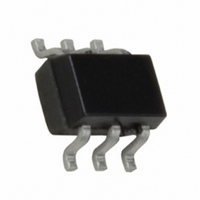
FDG6308P Fairchild Semiconductor, FDG6308P Datasheet - Page 4

FDG6308P
Manufacturer Part Number
FDG6308P
Description
MOSFET P-CH DUAL 20V SC70-6
Manufacturer
Fairchild Semiconductor
Series
PowerTrench®r
Datasheet
1.FDG6308P.pdf
(5 pages)
Specifications of FDG6308P
Fet Type
2 P-Channel (Dual)
Fet Feature
Logic Level Gate
Rds On (max) @ Id, Vgs
400 mOhm @ 600mA, 4.5V
Drain To Source Voltage (vdss)
20V
Current - Continuous Drain (id) @ 25° C
600mA
Vgs(th) (max) @ Id
1.5V @ 250µA
Gate Charge (qg) @ Vgs
2.5nC @ 4.5V
Input Capacitance (ciss) @ Vds
153pF @ 10V
Power - Max
300mW
Mounting Type
Surface Mount
Package / Case
SC-70-6, SC-88, SOT-363
Configuration
Dual
Transistor Polarity
P-Channel
Resistance Drain-source Rds (on)
0.4 Ohm @ 4.5 V
Forward Transconductance Gfs (max / Min)
2.1 S
Drain-source Breakdown Voltage
20 V
Gate-source Breakdown Voltage
+/- 8 V
Continuous Drain Current
0.6 A
Power Dissipation
300 mW
Maximum Operating Temperature
+ 150 C
Mounting Style
SMD/SMT
Minimum Operating Temperature
- 55 C
Rohs Compliant
Yes
Lead Free Status / RoHS Status
Lead free / RoHS Compliant
Available stocks
Company
Part Number
Manufacturer
Quantity
Price
Company:
Part Number:
FDG6308P
Manufacturer:
FAIRCHILD
Quantity:
30 000
Part Number:
FDG6308P
Manufacturer:
FAIRCHILD/ن»™ç«¥
Quantity:
20 000
Typical Characteristics
5
4
3
2
1
0
0.01
Figure 9. Maximum Safe Operating Area.
0.1
10
0
Figure 7. Gate Charge Characteristics.
1
0.1
R
SINGLE PULSE
R
0.001
I
D
DS(ON)
0.01
V
JA
= -0.6A
T
0.1
0.3
GS
A
0.0001
= 415
1
= 25
= -4.5V
LIMIT
o
o
C/W
C
D = 0.5
-V
0.6
0.2
DS
0.1
0.05
SINGLE PULSE
, DRAIN-SOURCE VOLTAGE (V)
Q
0.02
0.01
g
1
, GATE CHARGE (nC)
0.9
0.001
DC
1s
Figure 11. Transient Thermal Response Curve.
100ms
1.2
Thermal characterization performed using the conditions described in Note 1.
Transient thermal response will change depending on the circuit board design.
10ms
V
DS
= -5V
10
1ms
1.5
100 s
-15V
0.01
1.8
-10V
100
2.1
t
1
, TIME (sec)
0.1
200
160
120
30
24
18
12
0.0001
80
40
6
0
0
Figure 8. Capacitance Characteristics.
0
Figure 10. Single Pulse Maximum
0.001
4
-V
Power Dissipation.
1
DS
C
C
C
, DRAIN TO SOURCE VOLTAGE (V)
SINGLE PULSE TIME (SEC)
OSS
RSS
0.01
ISS
8
P(pk)
0.1
Duty Cycle, D = t
T
R
R
J
JA
- T
JA
10
(t) = r(t) + R
A
= 415 °C/W
t
12
1
= P * R
t
2
1
JA
SINGLE PULSE
R
1
(t)
JA
/ t
JA
T
FDG6308P Rev B (W)
2
16
A
10
= 415
= 25
V
f = 1MHz
GS
100
o
o
= 0 V
C
C/W
100
20


