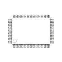
PCA9620H/Q900/1,51 NXP Semiconductors, PCA9620H/Q900/1,51 Datasheet - Page 51

PCA9620H/Q900/1,51
Manufacturer Part Number
PCA9620H/Q900/1,51
Description
LCD Drivers 480 SEGMENT LCD SEGMENT DRIVER
Manufacturer
NXP Semiconductors
Datasheet
1.PCA9620HQ900151.pdf
(71 pages)
Specifications of PCA9620H/Q900/1,51
Number Of Segments
60
Maximum Clock Frequency
14500 Hz
Operating Supply Voltage
2.5 V to 5.5 V
Maximum Power Dissipation
400 mW
Maximum Operating Temperature
+ 105 C
Package / Case
LQFP-80
Maximum Supply Current
200 uA
Minimum Operating Temperature
- 40 C
Lead Free Status / RoHS Status
Lead free / RoHS Compliant
Other names
935291899518
Available stocks
Company
Part Number
Manufacturer
Quantity
Price
Company:
Part Number:
PCA9620H/Q900/1,51
Manufacturer:
NXP Semiconductors
Quantity:
10 000
NXP Semiconductors
PCA9620
Product data sheet
Fig 47. I
EXAMPLES
a) transmit two bytes of RAM data
b) transmit two command bytes
c) transmit one command byte and two RAM date bytes
S 0 1 1 1 0
S 0 1 1 1 0
S 0 1 1 1 0
S 0 1 1 1 0
2
slave address
C-bus protocol write mode
8.5 I
8.6 Input filters
8.7 I
8.8 I
A
A
A
A
1
1
1
1
R/W = 0
A
A
A
A
0
0
0
0
0
0
0
0
The PCA9620 acts as an I
transmit data to an I
acknowledge signals and the temperature readout byte of the selected device.
To enhance noise immunity in electrically adverse environments, RC low-pass filters are
provided on the SDA and SCL lines.
Device selection depends on the I
Four different I
Table
Table 32.
The least significant bit of the slave address byte is bit R/W. Bit 1 and bit 2 of the slave
address are defined by connecting the inputs A0 and A1 to either V
(logic 1). Therefore, four instances of PCA9620 can be distinguished on the same
I
Bit
slave address
A
A
A
A
2
2
2
2
C-bus.
C-bus controller
C-bus slave address
C-bus protocol
C
O
0 1
1 0
1 0
R
S
control byte
32).
I
2
C slave address
2
C-bus slave addresses can be used to address the PCA9620 (see
All information provided in this document is subject to legal disclaimers.
A
A
A
A
M
S
B
RAM/command byte
2
C-bus master receiver. The only data output from PCA9620 are the
Slave address
7
MSB
0
RAM DATA
COMMAND
COMMAND
Rev. 1 — 9 December 2010
2
C-bus slave receiver. It does not initiate I
6
1
S
B
L
P
A
A
A
0 0
0 1
2
C-bus slave address.
RAM DATA
5
1
Universal LCD driver for low multiplex rates
4
1
A
A
A
P
COMMAND
RAM DATA
3
0
A
A
2
A1
P
SS
2
RAM DATA
C-bus transfers or
PCA9620
(logic 0) or V
© NXP B.V. 2010. All rights reserved.
1
A0
013aaa293
A
P
0
LSB
R/W
51 of 71
DD


