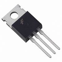
FDP8447L Fairchild Semiconductor, FDP8447L Datasheet - Page 2

FDP8447L
Manufacturer Part Number
FDP8447L
Description
MOSFET N-CH 40V 12A TO-220
Manufacturer
Fairchild Semiconductor
Series
PowerTrench®r
Datasheet
1.FDP8447L.pdf
(6 pages)
Specifications of FDP8447L
Fet Type
MOSFET N-Channel, Metal Oxide
Fet Feature
Logic Level Gate
Rds On (max) @ Id, Vgs
8.7 mOhm @ 14A, 10V
Drain To Source Voltage (vdss)
40V
Current - Continuous Drain (id) @ 25° C
12A
Vgs(th) (max) @ Id
3V @ 250µA
Gate Charge (qg) @ Vgs
49nC @ 10V
Input Capacitance (ciss) @ Vds
2500pF @ 20V
Power - Max
2W
Mounting Type
Through Hole
Package / Case
TO-220-3 (Straight Leads)
Configuration
Single
Transistor Polarity
N-Channel
Resistance Drain-source Rds (on)
0.0087 Ohms
Drain-source Breakdown Voltage
40 V
Gate-source Breakdown Voltage
+/- 20 V
Continuous Drain Current
12 A
Power Dissipation
2 W
Maximum Operating Temperature
+ 150 C
Mounting Style
Through Hole
Minimum Operating Temperature
- 55 C
Lead Free Status / RoHS Status
Lead free / RoHS Compliant
Available stocks
Company
Part Number
Manufacturer
Quantity
Price
Part Number:
FDP8447L
Manufacturer:
FAIRCHILD/ن»™ç«¥
Quantity:
20 000
©2007 Fairchild Semiconductor Corporation
FDP8447L Rev.B
Electrical Characteristics
Off Characteristics
On Characteristics
Dynamic Characteristics
Switching Characteristics
Drain-Source Diode Characteristics
NOTES:
1. R
2. Pulse Test: Pulse Width < 300µs, Duty cycle < 2.0%.
3. Starting T
BV
∆BV
I
I
V
r
g
C
C
C
R
t
t
t
t
Q
Q
Q
Q
V
t
Q
DSS
GSS
∆V
d(on)
r
d(off)
f
rr
DS(on)
R
FS
GS(th)
SD
∆T
∆T
iss
oss
rss
g
g
g
gs
gd
rr
Symbol
θJC
θJA
DSS
GS(th)
DSS
J
J
is the sum of the junction-to-case and case-to- ambient thermal resistance where the case thermal reference is defined as the solder mounting surface of the drain pins.
is guaranteed by design while R
J
= 25°C, L = 1mH, I
Drain to Source Breakdown Voltage
Breakdown Voltage Temperature
Coefficient
Zero Gate Voltage Drain Current
Gate to Source Leakage Current
Gate to Source Threshold Voltage
Gate to Source Threshold Voltage
Temperature Coefficient
Static Drain to Source On Resistance
Forward Transconductance
Input Capacitance
Output Capacitance
Reverse Transfer Capacitance
Gate Resistance
Turn-On Delay Time
Rise Time
Turn-Off Delay Time
Fall Time
Total Gate Charge
Total Gate Charge
Gate to Source Charge
Gate to Drain “Miller” Charge
Source to Drain Diode Forward Voltage
Reverse Recovery Time
Reverse Recovery Charge
AS
= 17.5A, V
θJA
Parameter
is determined by the user’s board design.
DD
= 40V, V
T
J
GS
= 25°C unless otherwise noted
= 10V.
V
V
V
V
V
f = 1MHz
f = 1MHz
I
I
V
V
V
I
V
V
V
V
V
I
D
D
D
F
DS
DD
GS
GS
GS
DS
GS
GS
GS
GS
GS
DD
GS
= 14A, di/dt = 100A/µs
= 250µA, V
= 250µA, referenced to 25°C
= 250µA, referenced to 25°C
= 0V to 10V
= 0V to 5V
= 20V, I
= 10V, R
= 32V,
= 20V, V
= 0V, I
= ±20V, V
= V
= 10V, I
= 4.5V, I
= 10V, I
= 5V, I
2
DS
Test Conditions
, I
S
D
D
D
D
= 14A
D
GS
GEN
= 14A
GS
= 14A,
D
DS
= 14A
= 14A, T
= 250µA
= 11A
= 0V,
= 0V
= 0V
= 6Ω
V
I
D
DD
(Note 2)
= 14A
J
= 20V,
= 125°C
Min
40
1
1880
12.1
Typ
245
150
1.7
7.7
8.9
1.4
4.7
6.2
0.8
34
74
28
35
19
28
22
-6
9
7
4
2500
±100
Max
13.7
11.2
325
225
8.7
1.2
18
14
45
10
49
27
42
33
www.fairchildsemi.com
1
3
mV/°C
mV/°C
Units
mΩ
µA
nA
pF
pF
pF
nC
nC
nC
nC
nC
ns
ns
ns
ns
ns
V
Ω
V
V
S


