FDC699P Fairchild Semiconductor, FDC699P Datasheet
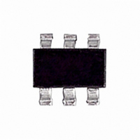
MOSFET P-CH 20V 7A SSOT-6

FDC699P

Manufacturer Part Number
FDC699P
Description
MOSFET P-CH 20V 7A SSOT-6
Manufacturer
Fairchild Semiconductor
Series
PowerTrench®r
Datasheet

Specifications of FDC699P

Fet Type
MOSFET P-Channel, Metal Oxide
Fet Feature
Logic Level Gate
Rds On (max) @ Id, Vgs
22 mOhm @ 7A, 4.5V
Drain To Source Voltage (vdss)
20V
Current - Continuous Drain (id) @ 25° C
7A
Vgs(th) (max) @ Id
1.5V @ 250µA
Gate Charge (qg) @ Vgs
38nC @ 5V
Input Capacitance (ciss) @ Vds
2640pF @ 10V
Power - Max
1.5W
Mounting Type
Surface Mount
Package / Case
6-SSOT FLMP, SuperSOT-6 FLMP
Lead Free Status / RoHS Status
Lead free / RoHS Compliant
Other names
FDC699PTR
FDC699P_NL
FDC699P_NLTR
FDC699P_NLTR

Available stocks

Company
Part Number
Manufacturer
Quantity
Price
Part Number:
FDC699P
Manufacturer:
FAIRCHILD
Quantity:
30 000
Part Number:
FDC699P
Manufacturer:
FAIRCHILD/仙童
Quantity:
20 000
FDC699P
P-Channel 2.5V PowerTrench
General Description
This P-Channel 2.5V specified MOSFET is a rugged
gate version of Fairchild Semiconductor’s advanced
PowerTrench process. It has been optimized for power
management applications with a wide range of gate
drive voltage (2.5V – 12V).
Applications
2004 Fairchild Semiconductor Corporation
Absolute Maximum Ratings
Symbol
V
V
I
P
T
Thermal Characteristics
R
R
Package Marking and Ordering Information
D
DSS
GSS
D
J
θJA
θJC
, T
Battery management
Load Switch
Battery protection
Device Marking
STG
.699
SuperSOT-6
Drain-Source Voltage
Gate-Source Voltage
Drain Current
Power Dissipation
Operating and Storage Junction Temperature Range
Thermal Resistance, Junction-to-Ambient
Thermal Resistance, Junction-to-Case
S
S
G
TM
FLMP
– Continuous
– Pulsed
FDC699P
Device
Parameter
S
S
S
T
A
MOSFET
=25
o
C unless otherwise noted
Reel Size
7’’
(Note 1a)
(Note 1a)
(Note 1b)
(Note 1a)
(Note 1b)
Features
• –7 A, –20 V
• High performance trench technology for extremely
• Fast switching speed
• FLMP SuperSOT-6 package: Enhanced thermal
low R
performance in industry-standard package size
1
2
3
DS(ON)
Tape width
R
R
DS(ON)
DS(ON)
–55 to +150
8mm
Ratings
Bottom Drain
–20
±12
–40
111
1.5
0.5
–7
60
2
= 22 mΩ @ V
= 30 mΩ @ V
5
6
4
January 2004
GS
GS
FDC699P Rev C2 (W)
3000 units
= –4.5 V
= –2.5 V
Quantity
Units
°C/W
°C
W
V
V
A

Related parts for FDC699P

FDC699P Summary of contents

Page 1

... Reel Size 7’’ January 2004 mΩ –4.5 V DS(ON mΩ –2.5 V DS(ON Bottom Drain Ratings Units –20 V ±12 V –7 A – 1.5 °C –55 to +150 °C/W 60 111 0.5 Tape width Quantity 8mm 3000 units FDC699P Rev C2 (W) ...

Page 2

... Min Typ Max Units –20 V –12 mV/°C µA –1 ±100 nA –0.6 –0.9 –1 mV/° mΩ =125° 2640 pF 560 pF 280 pF Ω 3 120 –1.6 A –0.7 –1.2 V (Note 111°C/W when mounted on a minimum pad copper FDC699P Rev C2 (W) ...

Page 3

... Dimensional Outline and Pad Layout Bottom View Top View Recommended Landing Pattern FDC699P Rev C2 (W) ...

Page 4

... Gate-to-Source Voltage. 100 0 0.001 0.0001 0 0.2 2.5 3 Figure 6. Body Diode Forward Voltage Variation with Source Current and Temperature. -2.5V -3.0V -3.5V -4.0V -4. DRAIN CURRENT ( -3. 125 GATE TO SOURCE VOLTAGE ( 125 -55 C 0.4 0.6 0 BODY DIODE FORWARD VOLTAGE (V) SD FDC699P Rev C2 ( 1.2 ...

Page 5

... Figure 10. Single Pulse Maximum 0.01 0 1MHz ISS C oss DRAIN TO SOURCE VOLTAGE (V) DS SINGLE PULSE R = 111°C/W θ 25° 100 1000 t , TIME (sec) 1 Power Dissipation. R ( θJA θ 111 °C/W θJA P(pk (t) θ Duty Cycle 100 1000 FDC699P Rev C2 (W) 20 ...

Page 6

... TRADEMARKS The following are registered and unregistered trademarks Fairchild Semiconductor owns or is authorized to use and is not intended exhaustive list of all such trademarks. ACEx™ FACT Quiet Series™ ActiveArray™ FAST Bottomless™ FASTr™ CoolFET™ FPS™ CROSSVOLT™ ...

Related keywords