NTD20N06L-001 ON Semiconductor, NTD20N06L-001 Datasheet

MOSFET N-CH 60V 20A TO-251A

NTD20N06L-001

Manufacturer Part Number
NTD20N06L-001
Description
MOSFET N-CH 60V 20A TO-251A
Manufacturer
ON Semiconductor
Datasheet

Specifications of NTD20N06L-001

Fet Type
MOSFET N-Channel, Metal Oxide
Fet Feature
Logic Level Gate
Rds On (max) @ Id, Vgs
48 mOhm @ 10A, 5V
Drain To Source Voltage (vdss)
60V
Current - Continuous Drain (id) @ 25° C
20A
Vgs(th) (max) @ Id
2V @ 250µA
Gate Charge (qg) @ Vgs
32nC @ 5V
Input Capacitance (ciss) @ Vds
990pF @ 25V
Power - Max
1.36W
Mounting Type
Surface Mount
Package / Case
IPak, TO-251, DPak, VPak (3 straight leads + tab)
Lead Free Status / RoHS Status
Contains lead / RoHS non-compliant
Other names
NTD20N06L-001OS

Available stocks

Company
Part Number
Manufacturer
Quantity
Price
Part Number:
NTD20N06L-001
Manufacturer:
ON
Quantity:
12 500
NTD20N06L
Power MOSFET
20 Amps, 60 Volts
Logic Level, N−Channel DPAK
power supplies, converters and power motor controls and bridge
circuits.
Features
Typical Applications
Maximum ratings are those values beyond which device damage can occur.
Maximum ratings applied to the device are individual stress limit values (not
normal operating conditions) and are not valid simultaneously. If these limits are
exceeded, device functional operation is not implied, damage may occur and
reliability may be affected.
1. When surface mounted to an FR4 board using 1 in pad size, (Cu Area 1.127 in
2. When surface mounted to an FR4 board using recommended pad size,
MAXIMUM RATINGS
© Semiconductor Components Industries, LLC, 2005
August, 2005 − Rev. 2
Drain−to−Source Voltage
Drain−to−Gate Voltage (R
Gate−to−Source Voltage
Drain Current
Total Power Dissipation @ T
Derate above 25°C
Total Power Dissipation @ T
Operating and Storage Temperature Range
Single Pulse Drain−to−Source Avalanche
Energy − Starting T
(V
L = 1.0 mH, I
Thermal Resistance
Maximum Lead Temperature for Soldering
Purposes, 1/8 in from case for 10 seconds
Designed for low voltage, high speed switching applications in
Pb−Free Packages are Available
Power Supplies
Converters
Power Motor Controls
Bridge Circuits
(Cu Area 0.412 in
DD
= 25 Vdc, V
L
(pk) = 16 A, V
− Junction−to−Case
− Junction−to−Ambient (Note 1)
− Junction−to−Ambient (Note 2)
− Continuous
− Non−repetitive (t
− Continuous @ T
− Continuous @ T
− Single Pulse (t
GS
Rating
J
2
= 5.0 Vdc,
).
= 25°C
(T
J
GS
= 25°C unless otherwise noted)
DS
A
A
A
= 10 MW)
= 25°C
= 25°C (Note 1)
= 25°C (Note 2)
= 60 Vdc)
p
v10 ms)
A
A
p
v10 ms)
= 25°C
= 100°C
Symbol
T
V
V
R
R
R
J
V
V
E
I
P
DGR
, T
T
DSS
I
I
DM
qJC
qJA
qJA
GS
GS
D
D
AS
D
L
stg
−55 to
Value
+175
"15
"20
0.40
1.88
1.36
128
260
110
2.5
60
60
20
10
60
60
80
1
W/°C
°C/W
Unit
Vdc
Vdc
Vdc
Adc
Apk
mJ
°C
°C
W
W
W
2
).
1 2
See detailed ordering and shipping information in the package
dimensions section on page 2 of this data sheet.
1
V
2
(BR)DSS
3
60 V
3
Y
WW
20N6L
G
ORDERING INFORMATION
4
4
G
http://onsemi.com
(Surface Mount)
(Straight Lead)
CASE 369C
CASE 369D
39 mW@5.0 V
STYLE 2
STYLE 2
R
N−Channel
DPAK
DPAK
DS(on)
= Year
= Work Week
= Device Code
= Pb−Free Package
D
Publication Order Number:
MARKING DIAGRAMS
& PIN ASSIGNMENTS
S
TYP
Gate
Gate
1
1
NTD20N06L/D
Drain
Drain
Drain
Drain
4
2
4
2
(Note 1)
I
D
20 A
MAX
3
Source
3
Source

Related parts for NTD20N06L-001

NTD20N06L-001 Summary of contents

Page 1

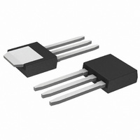
... G S MARKING DIAGRAMS & PIN ASSIGNMENTS 4 Drain 4 DPAK CASE 369C (Surface Mount) STYLE Drain Gate Source 4 Drain 4 DPAK CASE 369D (Straight Lead) STYLE Gate Drain Source Y = Year WW = Work Week 20N6L = Device Code G = Pb−Free Package ORDERING INFORMATION Publication Order Number: NTD20N06L/D ...

Page 2

... Switching characteristics are independent of operating junction temperatures. ORDERING INFORMATION Device NTD20N06L NTD20N06LG NTD20N06L−1 NTD20N06L−1G NTD20N06LT4 NTD20N06LT4G †For information on tape and reel specifications, including part orientation and tape sizes, please refer to our Tape and Reel Packaging Specifications Brochure, BRD8011/D. NTD20N06L (T = 25°C unless otherwise noted) J Symbol ...

Page 3

... DRAIN CURRENT (AMPS) D Figure 3. On−Resistance versus Gate−to−Source Voltage 1.8 GS 1.6 1.4 1.2 1 0.8 0.6 −50 − JUNCTION TEMPERATURE (°C) J Figure 5. On−Resistance Variation with Temperature NTD20N06L 40 ≥ 4 3 100° 1 GATE−TO−SOURCE VOLTAGE (VOLTS) GS Figure 2. Transfer Characteristics 0.085 0.075 ...

Page 4

... GATE−TO−SOURCE OR DRAIN−TO−SOURCE VOLTAGE (VOLTS) NTD20N06L POWER MOSFET SWITCHING The capacitance (C a voltage corresponding to the off−state condition when calculating t on−state when calculating t At high switching speeds, parasitic circuit elements complicate the analysis. The inductance of the MOSFET ...

Page 5

... In addition the total transition time ( power averaged over a complete switching cycle must not exceed (T − T )/(R ). qJC J(MAX Power MOSFET designated E−FET can be safely used in switching circuits with unclamped inductive loads. For NTD20N06L 1000 100 GS t d(off) ...

Page 6

... DRAIN−TO−SOURCE VOLTAGE (VOLTS) DS Figure 11. Maximum Rated Forward Biased Safe Operating Area 1 0.5 0.2 0.1 0.05 0.1 0.02 0.01 SINGLE PULSE 0.01 0.00001 0.0001 I Figure 14. Diode Reverse Recovery Waveform NTD20N06L SAFE OPERATING AREA 140 10 ms 120 100 100 STARTING JUNCTION TEMPERATURE (°C) J Figure 12 ...

Page 7

... 0.13 (0.005) M 5.80 0.228 *For additional information on our Pb−Free strategy and soldering details, please download the ON Semiconductor Soldering and Mounting Techniques Reference Manual, SOLDERRM/D. NTD20N06L PACKAGE DIMENSIONS DPAK CASE 369C−01 ISSUE O SEATING −T− PLANE SOLDERING FOOTPRINT* 6.20 3.0 0.244 ...

Page 8

... S 0.025 0.040 0.63 1.01 V 0.035 0.050 0.89 1.27 Z 0.155 −−− 3.93 −−− STYLE 2: PIN 1. GATE 2. DRAIN 3. SOURCE 4. DRAIN ON Semiconductor Website: http://onsemi.com Order Literature: http://www.onsemi.com/litorder For additional information, please contact your local Sales Representative. NTD20N06L/D ...

Related keywords