NTD20N06-1G ON Semiconductor, NTD20N06-1G Datasheet - Page 2
NTD20N06-1G
Manufacturer Part Number
NTD20N06-1G
Description
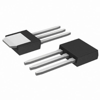
MOSFET N-CH 60V 20A IPAK
Manufacturer
ON Semiconductor
Datasheet
1.NTD20N06T4G.pdf
(7 pages)
Specifications of NTD20N06-1G
Fet Type
MOSFET N-Channel, Metal Oxide
Fet Feature
Standard
Rds On (max) @ Id, Vgs
46 mOhm @ 10A, 10V
Drain To Source Voltage (vdss)
60V
Current - Continuous Drain (id) @ 25° C
20A
Vgs(th) (max) @ Id
4V @ 250µA
Gate Charge (qg) @ Vgs
30nC @ 10V
Input Capacitance (ciss) @ Vds
1015pF @ 25V
Power - Max
1.36W
Mounting Type
Surface Mount
Package / Case
IPak, TO-251, DPak, VPak (3 straight leads + tab)
Lead Free Status / RoHS Status
Lead free / RoHS Compliant
Available stocks
Company
Part Number
Manufacturer
Quantity
Price
Company:

Part Number:
NTD20N06-1G
Manufacturer:
ON
Quantity:
12 500


3. Pulse Test: Pulse Width ≤ 300 ms, Duty Cycle ≤ 2%.
4. Switching characteristics are independent of operating junction temperatures.
†For information on tape and reel specifications, including part orientation and tape sizes, please refer to our Tape and Reel Packaging
ELECTRICAL CHARACTERISTICS
OFF CHARACTERISTICS
ON CHARACTERISTICS (Note 3)
DYNAMIC CHARACTERISTICS
SWITCHING CHARACTERISTICS (Note 4)
SOURCE−DRAIN DIODE CHARACTERISTICS
ORDERING INFORMATION
Specifications Brochure, BRD8011/D.
NTD20N06G
NTD20N06T4G
Drain−to−Source Breakdown Voltage (Note 3)
Temperature Coefficient (Positive)
Zero Gate Voltage Drain Current
Gate−Body Leakage Current (V
Gate Threshold Voltage (Note 3)
Threshold Temperature Coefficient (Negative)
Static Drain−to−Source On−Resistance (Note 3)
Static Drain−to−Source On−Voltage (Note 3)
Forward Transconductance (Note 3) (V
Input Capacitance
Output Capacitance
Transfer Capacitance
Turn−On Delay Time
Rise Time
Turn−Off Delay Time
Fall Time
Gate Charge
Forward On−Voltage
Reverse Recovery Time
Reverse Recovery Stored Charge
(V
(V
(V
(V
(V
(V
(V
GS
DS
DS
DS
GS
GS
GS
= 60 Vdc, V
= 60 Vdc, V
= V
= 0 Vdc, I
= 10 Vdc, I
= 10 Vdc, I
= 10 Vdc, I
GS
, I
D
D
= 250 mAdc)
D
D
D
= 250 mAdc)
GS
GS
Device
= 10 Adc)
= 20 Adc)
= 10 Adc, T
= 0 Vdc)
= 0 Vdc, T
Characteristic
GS
J
J
= 150°C)
= 150°C)
= ± 20 Vdc, V
(I
DS
(T
S
(I
S
= 20 Adc, V
J
= 7.0 Vdc, I
= 25°C unless otherwise noted)
= 20 Adc, V
(V
(V
(V
(I
dI
DS
S
DD
DS
V
S
DS
R
/dt = 100 A/ms) (Note 3)
GS
= 20 Adc, V
= 25 Vdc, V
G
= 30 Vdc, I
= 48 Vdc, I
V
= 0 Vdc)
= 10 Vdc) (Note 3)
= 9.1 W) (Note 3)
f = 1.0 MHz)
GS
GS
D
GS
= 6.0 Adc)
= 10 Vdc,
http://onsemi.com
= 0 Vdc, T
= 0 Vdc) (Note 3)
GS
D
D
GS
= 20 Adc,
= 20 Adc,
= 0 Vdc,
= 0 Vdc,
(Pb−Free)
(Pb−Free)
Package
DPAK
DPAK
2
J
= 150°C)
V
Symbol
R
V
V
(BR)DSS
t
t
I
I
C
Q
DS(on)
DS(on)
C
V
GS(th)
C
g
d(on)
d(off)
DSS
GSS
Q
Q
Q
t
t
t
FS
oss
t
t
SD
rss
RR
iss
rr
a
b
r
f
T
1
2
Min
2.0
60
−
−
−
−
−
−
−
−
−
−
−
−
−
−
−
−
−
−
−
−
−
−
−
−
−
2500 Tape & Reel
75 Units/Rail
0.084
71.7
79.4
2.91
37.5
0.78
1.57
13.2
60.5
27.1
37.1
21.2
0.87
42.9
Typ
725
213
Shipping
6.9
9.5
5.6
7.3
1.0
9.9
58
33
−
−
−
±100
1015
†
Max
1.10
300
120
120
1.0
4.0
1.2
10
46
20
60
80
30
−
−
−
−
−
−
−
−
−
−
−
−
mV/°C
mV/°C
mhos
mAdc
nAdc
Unit
Vdc
Vdc
Vdc
Vdc
mW
nC
mC
pF
ns
ns
Related parts for NTD20N06-1G
Image
Part Number
Description
Manufacturer
Datasheet
Request
R

Part Number:
Description:
ON Semiconductor [VOLTAGE REGULATOR]
Manufacturer:
ON Semiconductor
Datasheet:
Part Number:
Description:
357-036-542-201 CARDEDGE 36POS DL .156 BLK LOPRO
Manufacturer:
ON Semiconductor
Datasheet:
Part Number:
Description:
357-036-542-201 CARDEDGE 36POS DL .156 BLK LOPRO
Manufacturer:
ON Semiconductor
Datasheet:
Part Number:
Description:
357-036-542-201 CARDEDGE 36POS DL .156 BLK LOPRO
Manufacturer:
ON Semiconductor
Datasheet:
Part Number:
Description:
357-036-542-201 CARDEDGE 36POS DL .156 BLK LOPRO
Manufacturer:
ON Semiconductor
Datasheet:
Part Number:
Description:
357-036-542-201 CARDEDGE 36POS DL .156 BLK LOPRO
Manufacturer:
ON Semiconductor
Datasheet:
Part Number:
Description:
357-036-542-201 CARDEDGE 36POS DL .156 BLK LOPRO
Manufacturer:
ON Semiconductor
Datasheet:
Part Number:
Description:
357-036-542-201 CARDEDGE 36POS DL .156 BLK LOPRO
Manufacturer:
ON Semiconductor
Datasheet:
Part Number:
Description:
357-036-542-201 CARDEDGE 36POS DL .156 BLK LOPRO
Manufacturer:
ON Semiconductor
Datasheet:
Part Number:
Description:
357-036-542-201 CARDEDGE 36POS DL .156 BLK LOPRO
Manufacturer:
ON Semiconductor
Datasheet:
Part Number:
Description:
357-036-542-201 CARDEDGE 36POS DL .156 BLK LOPRO
Manufacturer:
ON Semiconductor
Datasheet:
Part Number:
Description:
Manufacturer:
ON Semiconductor
Datasheet:
Part Number:
Description:
Manufacturer:
ON Semiconductor
Datasheet:
Part Number:
Description:
Manufacturer:
ON Semiconductor
Datasheet: