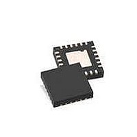
ISP1506BBS,557 NXP Semiconductors, ISP1506BBS,557 Datasheet - Page 21

ISP1506BBS,557
Manufacturer Part Number
ISP1506BBS,557
Description
RF Transceiver USB2.0 ULPI DDR OTG
Manufacturer
NXP Semiconductors
Datasheet
1.ISP1506BBS557.pdf
(80 pages)
Specifications of ISP1506BBS,557
Operating Supply Voltage
1.65 V to 3.6 V
Mounting Style
SMD/SMT
Package / Case
HVQFN-24
Lead Free Status / RoHS Status
Lead free / RoHS Compliant
Other names
935278349557 ISP1506BBS
NXP Semiconductors
9. Protocol description
ISP1506A_ISP1506B_2
Product data sheet
9.1 ULPI references
9.2 Power-On Reset (POR)
9.3 Power-up, reset and bus idle sequence
The following subsections describe the protocol for using the ISP1506.
Remark: In all figures, the ULPI data is shown in a generic form and not as nibbles on the
rising and falling edges of the clock.
The ISP1506 provides an 8-pin ULPI interface to communicate with the link. It is highly
recommended that you read
Rev. 1.1”
An internal POR is generated when REG1V8 rises above V
t
below V
voltage on REG1V8 is generated from V
To give a better view of the functionality,
internal POR starts with logic 0 at t0. At t1, the detector will see the passing of the trip
level so that POR turns to logic 1 and a delay element will add another t
drops to logic 0. If REG1V8 dips from t2 to t3 for > t
generated. If the dip at t4 to t5 is too short, that is, < t
will not react and will remain LOW.
Figure 6
On power-up, the ISP1506 performs an internal power-on reset and asserts DIR to
indicate to the link that the ULPI bus cannot be used. When the internal PLL is stable, the
ISP1506 deasserts DIR. The power-up time depends on the V
crystal start-up time, and PLL start-up time t
the ISP1506 drives the NXT pin to LOW and drives DATA[3:0] with RXCMD values. When
DIR is deasserted, the link must drive the data bus to a valid level. By default, the link
must drive data to LOW. When the ISP1506 initially deasserts DIR on power-up, the link
must ignore all RXCMDs until it resets the ISP1506. Before beginning USB packets, the
link must set the RESET bit in the Function Control register to reset the ISP1506. After the
RESET bit is set, the ISP1506 will assert DIR until the internal reset completes. The
ISP1506 will automatically deassert DIR and clear the RESET bit when reset has
w(REG1V8_H)
Fig 5.
POR(trip)
shows a typical start-up sequence.
Internal power-on reset timing
and
t0
. The internal POR pulse will also be generated whenever REG1V8 drops
Ref. 4 “UTMI+ Specification Rev.
for more than t
t1
t
PORP
Rev. 02 — 28 August 2008
Ref. 3 “UTMI+ Low Pin Interface (ULPI) Specification
w(REG1V8_L)
t2
Figure 5
CC
, and then rises above V
.
startup(o)(CLOCK)
ISP1506A; ISP1506B
t3
t
PORP
1.0”.
shows a possible curve of REG1V8. The
w(REG1V8_L)
w(REG1V8_L)
t4
ULPI HS USB OTG transceiver
. Whenever DIR is asserted,
POR(trip)
t5
CC
, another POR pulse is
, the internal POR pulse
supply rise time, the
POR(trip)
, for at least
© NXP B.V. 2008. All rights reserved.
004aaa751
PORP
REG1V8
V
POR
POR(trip)
again. The
before it
20 of 79


