PMBT3904M,315 NXP Semiconductors, PMBT3904M,315 Datasheet
PMBT3904M,315
Specifications of PMBT3904M,315
Available stocks


Related parts for PMBT3904M,315


PMBT3904M,315 Summary of contents
Page 1
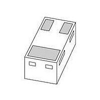
PMBT3904M 40 V, 200 mA NPN switching transistor Rev. 01 — 21 July 2009 BOTTOM VIEW 1. Product profile 1.1 General description NPN single switching transistor in a SOT883 (SC-101) leadless ultra small Surface-Mounted Device (SMD) plastic package. PNP complement: ...
Page 2
... NXP Semiconductors 3. Ordering information Table 3. Type number PMBT3904M 4. Marking Table 4. Type number PMBT3904M 5. Limiting values Table 5. In accordance with the Absolute Maximum Rating System (IEC 60134). Symbol V CBO V CEO V EBO tot amb T stg [1] Reflow soldering is the only recommended soldering method. ...
Page 3
... NXP Semiconductors (1) FR4 PCB, mounting pad for collector 1 cm (2) FR4 PCB, standard footprint Fig 1. 6. Thermal characteristics Table 6. Symbol R th(j-a) [1] Reflow soldering is the only recommended soldering method. [2] Device mounted on an FR4 PCB, single-sided copper, tin-plated and standard footprint. [3] Device mounted on an FR4 PCB, single-sided copper, tin-plated, mounting pad for collector 1 cm ...
Page 4
... NXP Semiconductors 3 10 duty cycle = 1 Z th(j-a) 0.75 (K/W) 0.5 0. 0.2 0.1 0.05 0. FR4 PCB, standard footprint Fig 2. Transient thermal impedance from junction to ambient as a function of pulse duration; typical values 7. Characteristics Table unless otherwise specified. amb Symbol I CBO ...
Page 5
... NXP Semiconductors Table unless otherwise specified. amb Symbol 600 h FE 400 (1) (2) 200 ( ( 150 C amb ( amb ( amb Fig 3. DC current gain as a function of collector current; typical values PMBT3904M_1 Product data sheet Characteristics …continued Parameter Conditions emitter capacitance V = 500 mV MHz C c transition frequency ...
Page 6
... NXP Semiconductors 1 (V) (1) 0.8 (2) ( amb ( amb ( 150 C amb Fig 5. Base-emitter voltage as a function of collector current; typical values ( 150 C amb ( amb ( amb Fig 7. Collector-emitter saturation voltage as a function of collector current; typical values PMBT3904M_1 Product data sheet 006aab117 V BEsat ( (mA) C (1) T (2) T (3) T Fig 6 ...
Page 7
... NXP Semiconductors 8. Test information Fig 8. 9. Package outline Fig 9. PMBT3904M_1 Product data sheet R (probe) oscilloscope 450 600 Oscilloscope: input impedance Test circuit for switching times 0.62 0.55 0.55 0.47 3 0.30 0.22 0.30 0. 0.20 0.12 0.35 Dimensions in mm Package outline SOT883 (SC-101) Rev. 01 — ...
Page 8
... NXP Semiconductors 10. Packing information Table 8. The indicated -xxx are the last three digits of the 12NC ordering code. Type number Package Description PMBT3904M [1] For further information and the availability of packing methods, see 11. Soldering 0.9 Fig 10. Reflow soldering footprint SOT883 (SC-101) PMBT3904M_1 ...
Page 9
... NXP Semiconductors 12. Revision history Table 9. Revision history Document ID Release date PMBT3904M_1 20090721 PMBT3904M_1 Product data sheet 40 V, 200 mA NPN switching transistor Data sheet status Change notice Product data sheet - Rev. 01 — 21 July 2009 PMBT3904M Supersedes - © NXP B.V. 2009. All rights reserved. ...
Page 10
... Right to make changes — NXP Semiconductors reserves the right to make changes to information published in this document, including without limitation specifications and product descriptions, at any time and without notice ...
Page 11
... NXP Semiconductors 15. Contents 1 Product profi 1.1 General description 1.2 Features . . . . . . . . . . . . . . . . . . . . . . . . . . . . . . 1 1.3 Applications . . . . . . . . . . . . . . . . . . . . . . . . . . . 1 1.4 Quick reference data Pinning information . . . . . . . . . . . . . . . . . . . . . . 1 3 Ordering information . . . . . . . . . . . . . . . . . . . . . 2 4 Marking . . . . . . . . . . . . . . . . . . . . . . . . . . . . . . . . 2 5 Limiting values Thermal characteristics Characteristics . . . . . . . . . . . . . . . . . . . . . . . . . . 4 8 Test information . . . . . . . . . . . . . . . . . . . . . . . . . 7 9 Package outline . . . . . . . . . . . . . . . . . . . . . . . . . 7 10 Packing information Soldering . . . . . . . . . . . . . . . . . . . . . . . . . . . . . . 8 12 Revision history ...