MJE243G ON Semiconductor, MJE243G Datasheet - Page 3
MJE243G
Manufacturer Part Number
MJE243G
Description
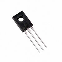
TRANS PWR NPN 4A 100V TO225AA
Manufacturer
ON Semiconductor
Type
Powerr
Specifications of MJE243G
Transistor Type
NPN
Current - Collector (ic) (max)
4A
Voltage - Collector Emitter Breakdown (max)
100V
Vce Saturation (max) @ Ib, Ic
600mV @ 100mA, 1A
Dc Current Gain (hfe) (min) @ Ic, Vce
40 @ 200mA, 1V
Power - Max
1.5W
Frequency - Transition
40MHz
Mounting Type
Through Hole
Package / Case
TO-225-3
Transistor Polarity
NPN
Mounting Style
Through Hole
Collector- Emitter Voltage Vceo Max
100 V
Emitter- Base Voltage Vebo
7 V
Maximum Dc Collector Current
4 A
Power Dissipation
15 W
Maximum Operating Temperature
+ 150 C
Continuous Collector Current
4 A
Dc Collector/base Gain Hfe Min
40
Maximum Operating Frequency
40 MHz
Minimum Operating Temperature
- 65 C
Current, Collector
4 A
Current, Gain
15
Frequency
40 MHz
Package Type
TO-225
Polarity
NPN
Primary Type
Si
Resistance, Thermal, Junction To Case
8.34 °C/W
Voltage, Breakdown, Collector To Emitter
100 V
Voltage, Collector To Base
100 V
Voltage, Collector To Emitter
100 V
Voltage, Collector To Emitter, Saturation
0.6 V
Voltage, Emitter To Base
7 V
Number Of Elements
1
Collector-emitter Voltage
100V
Collector-base Voltage
100V
Emitter-base Voltage
7V
Collector Current (dc) (max)
4A
Dc Current Gain (min)
40
Frequency (max)
40MHz
Operating Temp Range
-65C to 150C
Operating Temperature Classification
Military
Mounting
Through Hole
Pin Count
3 +Tab
Lead Free Status / RoHS Status
Lead free / RoHS Compliant
Current - Collector Cutoff (max)
-
Lead Free Status / Rohs Status
Lead free / RoHS Compliant
Other names
MJE243GOS
Available stocks
Company
Part Number
Manufacturer
Quantity
Price

Company:
Part Number:
MJE243G
Manufacturer:
ON Semiconductor
Quantity:
450


+11 V
0
DUTY CYCLE = 1.0%
0.07
0.05
0.03
0.02
0.01
1.0
0.7
0.5
0.3
0.2
0.1
- 9.0 V
t
0.02
r
, t
f
≤ 10 ns
R
FOR PNP TEST CIRCUIT, REVERSE ALL POLARITIES
B
0 (SINGLE PULSE)
Figure 2. Switching Time Test Circuit
D
and R
1
0.05
1N5825 USED ABOVE I
MSD6100 USED BELOW I
25 ms
MUST BE FAST RECOVERY TYPE, e.g.:
D = 0.5
C
0.2
0.05
VARIED TO OBTAIN DESIRED CURRENT LEVELS
0.1
0.01
51
0.1
0.02
R
B
B
8.0
4.0
16
12
≈ 100 mA
B
0
20
≈ 100 mA
- 4 V
0.2
D
1
40
+ 30 V
V
CC
0.5
R
Figure 1. Power Derating
C
60
Figure 4. Thermal Response
http://onsemi.com
T, TEMPERATURE (°C)
SCOPE
1.0
80
t, TIME (ms)
3
100
2.0
500
300
200
100
q
q
D CURVES APPLY FOR POWER
PULSE TRAIN SHOWN
READ TIME AT t
T
1K
50
30
20
10
JC
JC
J(pk)
5
3
2
1
0.01
(t) = r(t) q
= 8.34°C/W MAX
- T
120
C
0.02
NPN MJE243
PNP MJE253
= P
JC
0.03 0.05
5.0
(pk)
1
140
q
JC
I
C
(t)
Figure 3. Turn−On Time
, COLLECTOR CURRENT (AMPS)
10
0.1
160
t
r
t
1.6
1.2
0.8
0.4
0
d
0.2
20
0.3
P
(pk)
DUTY CYCLE, D = t
0.5
t
1
1
t
2
50
V
I
T
C
J
CC
/I
= 25°C
B
2
= 30 V
= 10
3
1
/t
100
2
5
10
200
Related parts for MJE243G
Image
Part Number
Description
Manufacturer
Datasheet
Request
R

Part Number:
Description:
ON Semiconductor [VOLTAGE REGULATOR]
Manufacturer:
ON Semiconductor
Datasheet:
Part Number:
Description:
357-036-542-201 CARDEDGE 36POS DL .156 BLK LOPRO
Manufacturer:
ON Semiconductor
Datasheet:
Part Number:
Description:
357-036-542-201 CARDEDGE 36POS DL .156 BLK LOPRO
Manufacturer:
ON Semiconductor
Datasheet:
Part Number:
Description:
357-036-542-201 CARDEDGE 36POS DL .156 BLK LOPRO
Manufacturer:
ON Semiconductor
Datasheet:
Part Number:
Description:
357-036-542-201 CARDEDGE 36POS DL .156 BLK LOPRO
Manufacturer:
ON Semiconductor
Datasheet:
Part Number:
Description:
357-036-542-201 CARDEDGE 36POS DL .156 BLK LOPRO
Manufacturer:
ON Semiconductor
Datasheet:
Part Number:
Description:
357-036-542-201 CARDEDGE 36POS DL .156 BLK LOPRO
Manufacturer:
ON Semiconductor
Datasheet:
Part Number:
Description:
357-036-542-201 CARDEDGE 36POS DL .156 BLK LOPRO
Manufacturer:
ON Semiconductor
Datasheet:
Part Number:
Description:
357-036-542-201 CARDEDGE 36POS DL .156 BLK LOPRO
Manufacturer:
ON Semiconductor
Datasheet:
Part Number:
Description:
357-036-542-201 CARDEDGE 36POS DL .156 BLK LOPRO
Manufacturer:
ON Semiconductor
Datasheet:
Part Number:
Description:
357-036-542-201 CARDEDGE 36POS DL .156 BLK LOPRO
Manufacturer:
ON Semiconductor
Datasheet:
Part Number:
Description:
Manufacturer:
ON Semiconductor
Datasheet:
Part Number:
Description:
Manufacturer:
ON Semiconductor
Datasheet:
Part Number:
Description:
Manufacturer:
ON Semiconductor
Datasheet: