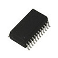
CAT5401WI-00-TE13 ON Semiconductor, CAT5401WI-00-TE13 Datasheet - Page 10

CAT5401WI-00-TE13
Manufacturer Part Number
CAT5401WI-00-TE13
Description
Manufacturer
ON Semiconductor
Datasheet
1.CAT5401WI-00-TE13.pdf
(16 pages)
Specifications of CAT5401WI-00-TE13
Number Of Elements
4
# Of Taps
64
Resistance (max)
100KOhm
Power Supply Requirement
Single
Interface Type
Serial (SPI)
Single Supply Voltage (typ)
3.3/5V
Dual Supply Voltage (typ)
Not RequiredV
Single Supply Voltage (min)
2.5V
Single Supply Voltage (max)
6V
Dual Supply Voltage (min)
Not RequiredV
Dual Supply Voltage (max)
Not RequiredV
Operating Temp Range
-40C to 85C
Operating Temperature Classification
Industrial
Mounting
Surface Mount
Pin Count
24
Lead Free Status / RoHS Status
Compliant
when set to "1" signifies a write cycle is in progress.
The basic sequence of the three byte instructions is
illustrated in Figure 8. These three-byte instructions
exchange data between the WCR and one of the Data
Registers. The WCR controls the position of the wiper.
The response of the wiper to this action will be delayed
by t
to a Data Register is a write to non-volatile memory and
takes a minimum of t
occur between one of the four potentiometers and one
of its associated registers; or the transfer can occur
between all potentiometers and one associated register.
Four instructions require a two-byte sequence to
complete, as illustrated in Figure 7. These instructions
transfer data between the host/processor and the
CAT5401; either between the host and one of the data
registers or directly between the host and the Wiper
Control Register. These instructions are:
— XFR Data Register to Wiper Control Register
— XFR Wiper Control Register to Data Register
— Global XFR Data Register to Wiper
Figure 7. Two-Byte Instruction Sequence
Document No. 2010, Rev. F
Figure 9. Increment/Decrement Instruction Sequence
Figure 8. Three-Byte Instruction Sequence
SI
This transfers the contents of one specified Data
Register to the associated Wiper Control Register.
This transfers the contents of the specified Wiper
Control Register to the specified associated
Data Register.
WRL
. A transfer from the WCR (current wiper position),
ID3 ID2 ID1 ID0
SI
0
Device ID
1
ID3 ID2 ID1 ID0
0
SI
Device ID
0
1
WR
1
0
A3
ID3 ID2 ID1 ID0
to complete. The transfer can
0
1
Device ID
A2
A3
1
Internal
Address
A1
Internal
Address
0
A2 A1 A0
1
A0
A3
I3
0
A2
Instruction
Opcode
I3
0
Internal
Address
I2
A1
Instruction
Opcode
I1
I2
A0
I0
I1
10
I3
I0
R1 R0
Data
Register
Address
Instruction
— Global XFR Wiper Counter Register to
INCREMENT/DECREMENT COMMAND
The final command is Increment/Decrement (Figure 5
and 9). The Increment/Decrement command is different
from the other commands. Once the command is issued
the master can clock the selected wiper up and/or down
in one segment steps; thereby providing a fine tuning
capability to the host. For each SCK clock pulse (t
while SI is HIGH, the selected wiper will move one
resistor segment towards the R
each SCK clock pulse while SI is LOW, the selected
wiper will move one resistor segment towards the R
terminal.
See Instructions format for more detail.
Opcode
I2
Data
Register
Address
R1
Control Register
This transfers the contents of all specified Data
Registers to the associated Wiper Control
Registers.
Data Register
This transfers the contents of all Wiper Control
Registers to the specified associated Data
Registers.
I1
R0 P1 P0
Address
P1 P0
Pot/WCR
I0
Pot/WCR
Address
Register
Address
R1 R0 P1
D7
N
C
1
I
D6 D5 D4 D3 D2
N
C
2
Data Register D[7:0]
I
Pot/WCR
Address
P0
Characteristics subject to change without notice
WCR[7:0]
N
C
n
I
or
H
terminal. Similarly, for
D
E
C
1
© Catalyst Semiconductor, Inc.
D1 D0
D
E
C
n
HIGH
L
)


