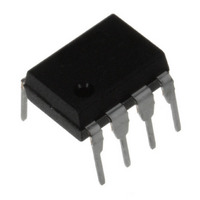
NJM567D NJR, NJM567D Datasheet - Page 5

NJM567D
Manufacturer Part Number
NJM567D
Description
IC TONE-DECODER/PH-LCKDLOOP 8DIP
Manufacturer
NJR
Type
Phase Lock Loop (PLL)r
Datasheet
1.NJM567D.pdf
(10 pages)
Specifications of NJM567D
Pll
Yes
Input
Clock
Output
Clock
Number Of Circuits
1
Ratio - Input:output
1:1
Differential - Input:output
No/No
Frequency - Max
500kHz
Divider/multiplier
No/No
Voltage - Supply
4.75 V ~ 9 V
Operating Temperature
-40°C ~ 85°C
Mounting Type
Through Hole
Package / Case
8-DIP
Frequency-max
500kHz
Lead Free Status / RoHS Status
Contains lead / RoHS non-compliant
Available stocks
Company
Part Number
Manufacturer
Quantity
Price
Part Number:
NJM567D
Manufacturer:
JRC
Quantity:
20 000
■ DESIGN FORMULAS
■ PLL WORDS EXPLANATIONS
will cause a logical zero state on the output. The detection bandwidth corresponds to the loop capture range.
the output.
- 2f
reduced to zero if necessary by means of an optional centering adjustment.
be sufficient for choosing the external components R
1. Select R
ohm, and the combined temperature coefficient of the R
temperature range to meet the necessary requirements.
2. Select the low pass capacitor, C
amplitude variation is known, the appropriate value of f
Conversely, an area of operation may be selected on this graph and the input level and C
For example, constant bandwidth operation requires that input amplitude be above 200mVrms. The bandwidth, as noted
on the graph, is then controlled solely by the f
3. The value of C
the detection band to eliminate spurious outputs. If C
output stage on and off at the beat frequency, or the output may pulse on and off during the turn-on transient. If C
large, turn-on and turn-off of the output stage will be delayed until the voltage on C
delay may be desirable to avoid spurious outputs due to transient frequencies.) A typical minimum value for C
Ver.2003-12-09
☆ Center Frequency (f
☆ Detection Bandwidth (BW)
☆ Lock Range
☆ Detection Band Skew
◎ Operating Instructions
The free-running frequency of the current controlled oscillator (CCO) in the absence of an input signal.
The frequency range, centered about f
The largest frequency range within which an input signal above the threshold voltage will hold a logical zero state on
A measure of how well the detection band is centered about the center frequency, f
Figure 1 shows a typical connection diagram for the 567. For most applications, the following three-step procedure will
O
where
)/ 2f
BW
f
O
=
O
~
−
1.07R
where f
1070
1
and C
V
C
1
IN
2
1
C
3
f
: Input Voltage (Vrms)
: LPF Capacitor (µF)
max
1
is generally non-critical. C
O
V
1
(
C
IN
for the desired center frequency. For best temperature stability, R
V
and f
2
IN
in
O
=
)
%
0
min
mV
of
are the frequencies corresponding to the edges of the detection band. The skew can be
f
O
)
V ,
IN
2
, by referring to the Bandwidth versus Input Signal Amplitude graph. If the input
≤
200
O
, within which an input signal above the threshold voltage (typically 20mVrms)
mVrms
3
O
sets the band edge of a low pass filter which attenuates frequencies outside
C
2
product (f
3
1
is too small, frequencies just outside the detection band will switch the
, C
Figure 1
1
O
C
1
2
C
C
O
and C
2
1
(Hz), C
product should have sufficient stability over the projected
necessary to give the desired bandwidth may be found.
3
.
2
(µfd)).
3
passes the threshold voltage. (Such
O
. The skew is defined as (f
1
should be between 2K and 20K
2
may be adjusted accordingly.
3
is 2C
max
2
.
3
- 5 -
is too
+ f
min


