MC14536B
Programmable Timer
counter with 16 stages selectable by a binary code. Provisions for an
on−chip RC oscillator or an external clock are provided. An on−chip
monostable circuit incorporating a pulse−type output has been
included. By selecting the appropriate counter stage in conjunction
with the appropriate input clock frequency, a variety of timing can be
achieved.
Features
•
•
•
•
•
•
•
•
•
•
•
•
Stresses exceeding Maximum Ratings may damage the device. Maximum
Ratings are stress ratings only. Functional operation above the Recommended
Operating Conditions is not implied. Extended exposure to stresses above the
Recommended Operating Conditions may affect device reliability.
1. Temperature Derating:
static voltages or electric fields. However, precautions must be taken to avoid
applications of any voltage higher than maximum rated voltages to this
high−impedance circuit. For proper operation, V
to the range V
(e.g., either V
*For additional information on our Pb−Free strategy and soldering details, please
© Semiconductor Components Industries, LLC, 2006
MAXIMUM RATINGS
download the ON Semiconductor Soldering and Mounting Techniques
Reference Manual, SOLDERRM/D.
DC Supply Voltage Range
Input or Output Voltage Range
(DC or Transient)
Input or Output Current
(DC or Transient) per Pin
Power Dissipation per Package (Note 1)
Ambient Temperature Range
Storage Temperature Range
Lead Temperature, (8−Second Soldering)
The MC14536B programmable timer is a 24−stage binary ripple
This device contains protection circuitry to guard against damage due to high
Unused inputs must always be tied to an appropriate logic voltage level
and Fall Times
Schottky TTL Load over the Rated Temperature Range
24 Flip−Flop Stages − Will Count From 2
Last 16 Stages Selectable By Four−Bit Select Code
8−Bypass Input Allows Bypassing of First Eight Stages
Set and Reset Inputs
Clock Inhibit and Oscillator Inhibit Inputs
On−Chip RC Oscillator Provisions
On−Chip Monostable Output Provisions
Clock Conditioning Circuit Permits Operation with Very Long Rise
Test Mode Allows Fast Test Sequence
Supply Voltage Range = 3.0 Vdc to 18 Vdc
Capable of Driving Two Low−Power TTL Loads or One Low−Power
Pb−Free Packages are Available*
Plastic “P and D/DW” Packages: – 7.0 mW/_C from 65_C to 125_C
SS
SS
or V
Rating
v (V
DD
in
). Unused outputs must be left open.
or V
(Voltages Referenced to V
out
) v V
DD
.
Symbol
I
in
V
V
V
T
P
, I
T
T
DD
out
stg
in
in
D
A
L
out
,
and V
0
to 2
SS
−0.5 to V
out
−0.5 to +18.0
)
−55 to +125
−65 to +150
24
should be constrained
Value
± 10
500
260
DD
+ 0.5
1
Unit
mW
mA
°C
°C
°C
V
V
See detailed ordering and shipping information in the package
dimensions section on page 12 of this data sheet.
1
1
1
A
WL, L
YY, Y
WW, W = Work Week
G
ORDERING INFORMATION
SOIC−16 WB
DW SUFFIX
CASE 751G
SOEIAJ−16
CASE 648
CASE 966
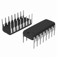
P SUFFIX
F SUFFIX
PDIP−16
= Assembly Location
= Wafer Lot
= Year
= Pb−Free Package
Publication Order Number:
1
1
1
MC14536BCP
AWLYYWWG
DIAGRAMS
AWLYWWG
MC14536B
MARKING
ALYWG
14536B
MC14536B/D