DS1646P-120+ Maxim Integrated Products, DS1646P-120+ Datasheet
DS1646P-120+
Specifications of DS1646P-120+


Related parts for DS1646P-120+

DS1646P-120+ Summary of contents
Page 1
... Underwriters Laboratories (UL) Recognized ORDERING INFORMATION VOLTAGE PART RANGE (V) DS1646-120+ 5.0 DS1646P-120+ 5.0 +Denotes a lead(Pb)-free/RoHS-compliant package. *DS9034-PCX+ or DS9034I-PCX+ required (must be ordered separately). A “+" indicates a lead(Pb)-free product. The top mark will include a “+" symbol on lead(Pb)-free devices. DS1646/DS1646P Nonvolatile Timekeeping RAM PIN CONFIGURATIONS N ...
Page 2
... V BAT FUNCTION No Connection Address Input Data Input/Output Ground Active-Low Chip Enable Address Input Active-Low Output Enable Active-Low Write Enable Address Input Power-Supply Input Active-Low Power-Fail Output, Open Drain. Requires a pullup resistor for proper operation. Crystal Connection, V Battery Connection BAT DS1646/DS1646P ...
Page 3
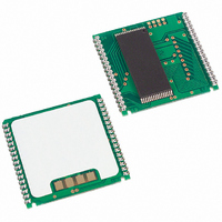
... This design allows the PowerCap to be mounted on top of the DS1646P after the completion of the surface mount process. Mounting the PowerCap after the surface mount process prevents damage to the crystal and battery due to the high temperatures required for solder reflow ...
Page 4
... V V READ DESELECT X X DESELECT bit is the MSB for the second’s registers. Setting it OSC low, and address for seconds register remain valid and stable DS1646/DS1646P DQ POWER HIGH-Z STANDBY HIGH-Z STANDBY DATA IN ACTIVE DATA OUT ACTIVE HIGH-Z ACTIVE HIGH-Z CMOS STANDBY ...
Page 5
... AA or access times are not met, valid data will output enable access time (t CEA and . If the outputs are activated before the address inputs are changed while DS1646/DS1646P FUNCTION — — Year — — Month — — Date — ...
Page 6
... DS1646 can be accessed as described above with CC is below the power-fail point V CC signal. At this time the power-fail output signal ( CE returns to nominal levels. When DS1646/DS1646P and . The addresses must be held valid CE prior to the initiation low prior to OE goes active. ...
Page 7
... OUT Power-Fail Voltage TEMPERATURE SYMBOL MIN -0.3 IL SYMBOL MIN I CC1 I ) CC2 IH I CC3 2 4 DS1646/DS1646P ±10% (Over the Operating Range) TYP MAX UNITS NOTES 5 0.8 V (Over the Operating Range) TYP MAX UNITS NOTES 4.0 mA µA +1 µ 0.4 V 4.25 4 ...
Page 8
... WEW t WEZ DH1 t 25 DH2 SYMBOL MIN SYMBOL MIN Fall Time t 300 Rise Time REC DS1646/DS1646P (Over the Operating Range) TYP MAX UNITS NOTES ns 120 ns 120 100 +25°C) A TYP MAX UNITS NOTES (Over the Operating Range) TYP MAX UNITS NOTES µs µ ...
Page 9
... DS1646 READ CYCLE TIMING DS1646 WRITE CYCLE TIMING DS1646/DS1646P ...
Page 10
... POWER-DOWN/POWER-UP TIMING OUTPUT LOAD DS1646/DS1646P ...
Page 11
... RoHS status only. Package drawings may show a different suffix character, but the drawing pertains to the package regardless of RoHS status. PACKAGE TYPE PACKAGE CODE 32 EDIP 34 PCAP going high. WE going high. CE OUTLINE NO. MDF32+1 21-0245 PC2+6 21-0246 DS1646/DS1646P Note LAND PATTERN NO. — — ...
Page 12
... Maxim cannot assume responsibility for use of any circuitry other than circuitry entirely embodied in a Maxim product. No circuit patent licenses are implied. Maxim reserves the right to change the circuitry and specifications without notice at any time © 2010 Maxim Integrated Products DESCRIPTION Maxim and the Dallas logo are a registered trademark of Maxim Integrated Products, Inc. DS1646/DS1646P PAGES CHANGED 1, 7 ...