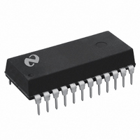
DP8572AN National Semiconductor, DP8572AN Datasheet - Page 11

DP8572AN
Manufacturer Part Number
DP8572AN
Description
IC REAL TIME CLOCK W/RAM 24 DIP
Manufacturer
National Semiconductor
Type
Clock/Calendar/NVSRAMr
Datasheet
1.DP8572AN.pdf
(22 pages)
Specifications of DP8572AN
Memory Size
44B
Time Format
HH:MM:SS:hh (12/24 hr)
Date Format
YY-MM-DD-dd
Interface
Parallel
Voltage - Supply
4.5 V ~ 5.5 V
Operating Temperature
-40°C ~ 85°C
Mounting Type
Through Hole
Package / Case
24-DIP (0.300", 7.62mm)
Lead Free Status / RoHS Status
Contains lead / RoHS non-compliant
Other names
*DP8572AN
DP8572
DP8572
Available stocks
Company
Part Number
Manufacturer
Quantity
Price
Part Number:
DP8572AN
Manufacturer:
TOSHIBA/东芝
Quantity:
20 000
Functional Description
Interrupts Fall Into Three Categories
1 The Alarm Compare Interrupt Issued when the value in
2 The Periodic Interrupts These are issued at every incre-
3 The Power Fail Interrupt Issued upon recognition of a
ALARM COMPARE INTERRUPT DESCRIPTON
The alarm time comparison interrupt is a special interrupt
similar to an alarm clock wake up buzzer This interrupt is
generated when the clock time is equal to a value pro-
grammed into the alarm compare registers Up to six bytes
can be enabled to perform alarm time comparisons on the
counter chain These six bytes or some subset thereof
would be loaded with the future time at which the interrupt
will occur Next the appropriate bits in the Interrupt Control
Register 1 are enabled or disabled (refer to detailed descrip-
tion of Interrupt Control Register 1) The RTC then com-
pares these bytes with the clock time When all the enabled
compare registers equal the clock time an alarm interrupt is
issued but only if the alarm compare interrupt is enabled
can the interrupt be generated externally Each alarm com-
pare bit in the Control Register will enable a specific byte for
comparison to the clock Disabling a compare byte is the
same as setting its associated counter comparator to an
‘‘always equal’’ state For example to generate an interrupt
at 3 15 AM of every day load the hours compare with 0 3
(BCD) the minutes compare with 1 5 (BCD) and the faster
counters with 0 0 (BCD) and then disable all other compare
registers So every day when the time rolls over from
3 14 59 99 an interrupt is issued This bit may be reset by
writing a one to bit D3 in the Main Status Register at any
time after the alarm has been generated
If time comparison for an individual byte counter is disabled
that corresponding RAM location can then be used as gen-
eral purpose storage
PERIODIC INTERRUPTS DESCRIPTION
The Periodic Flag Register contains six flags which are set
by real-time generated ‘‘ticks’’ at various time intervals see
the time compared RAM equals the counter
ment of the specific clock counter signal Thus an inter-
rupt is issued every minute second etc Each of these
interrupts occurs at the roll-over of the specific counter
power fail condition by the internal sensing logic The
power failed condition is determined by the signal on the
PFAIL pin The internal power fail signal is gated with the
chip select signal to ensure that the power fail interrupt
does not lock the chip out during a read or write
(Continued)
11
Figure 5 These flags constantly sense the periodic signals
and may be used whether or not interrupts are enabled
These flags are cleared by any read or write operation per-
formed on this register
To generate periodic interrupts at the desired rate the asso-
ciated Periodic Interrupt Enable bit in Interrupt Control Reg-
ister 0 must be set Any combination of periodic interrupts
may be enabled to operate simultaneously Enabled period-
ic interrupts will now affect the Periodic Interrupt Flag in the
Main Status Register
When a periodic event occurs the Periodic Interrupt Flag in
the Main Status Register is set causing an interrupt to be
generated The P clears both flag and interrupt by writing a
‘‘1’’ to the Periodic Interrupt Flag The individual flags in the
periodic Interrupt Flag Register do not require clearing to
cancel the interrupt
If all periodic interrupts are disabled and a periodic interrupt
is left pending (i e the Periodic Interrupt Flag is still set) the
Periodic Interrupt Flag will still be required to be cleared to
cancel the pending interrupt
POWER FAIL INTERRUPTS DESCRIPTION
The Power Fail Status Flag in the Main Status Register
monitors the state of the internal power fail signal This flag
may be interrogated by the P but it cannot be cleared it is
cleared automatically by the RTC when system power is
restored To generate an interrupt when the power fails the
Power Fail Interrupt Enable bit in Interrupt Control Register
1 is set Although this interrupt may not be cleared it may
be masked by clearing the Power Fail Interrupt Enable bit
POWER FAILURE CIRCUITRY FUNCTIONAL
DESCRIPTION
Since the clock must be operated from a battery when the
main system supply has been turned off the DP8572A pro-
vides circuitry to simplify design in battery backed systems
This switches over to the back up supply and isolates itself
from the host system Figure 6 shows a simplified block
diagram of this circuitry which consists of three major sec-
tions 1) power loss logic 2) battery switch over logic and 3)
isolation logic
Detection of power loss occurs when PFAIL is low De-
bounce logic provides a 30 s–63 s debounce time which
will prevent noise on the PFAIL pin from being interpreted
as a system failure After 30 s–63 s the debounce logic
times out and a signal is generated indicating that system
power is marginal and is failing The Power Fail Interrupt will
then be generated


