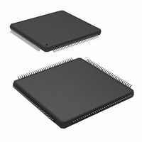
ADC08D500CIYB/NOPB National Semiconductor, ADC08D500CIYB/NOPB Datasheet - Page 7

ADC08D500CIYB/NOPB
Manufacturer Part Number
ADC08D500CIYB/NOPB
Description
IC ADC 8BIT 500MSPS DUAL 128LQFP
Manufacturer
National Semiconductor
Series
PowerWise®r
Specifications of ADC08D500CIYB/NOPB
Number Of Bits
8
Sampling Rate (per Second)
500M
Data Interface
Serial
Number Of Converters
2
Power Dissipation (max)
1.78W
Voltage Supply Source
Single Supply
Operating Temperature
-40°C ~ 85°C
Mounting Type
Surface Mount
Package / Case
128-LQFP Exposed Pad
Lead Free Status / RoHS Status
Lead free / RoHS Compliant
Other names
*ADC08D500CIYB
*ADC08D500CIYB/NOPB
ADC08D500CIYB
*ADC08D500CIYB/NOPB
ADC08D500CIYB
Available stocks
Company
Part Number
Manufacturer
Quantity
Price
Company:
Part Number:
ADC08D500CIYB/NOPB
Manufacturer:
Texas Instruments
Quantity:
10 000
STATIC CONVERTER CHARACTERISTICS
INL
DNL
V
V
PFSE
NFSE
FS_ADJ
NORMAL MODE (non DES) DYNAMIC CONVERTER CHARACTERISTICS
FPBW
B.E.R.
ENOB
SINAD
Symbol
OFF
OFF
Absolute Maximum Ratings
2)
If Military/Aerospace specified devices are required,
please contact the National Semiconductor Sales Office/
Distributors for availability and specifications.
Converter Electrical Characteristics
The following specifications apply after calibration for V
870mV
Floating, Non-Extended Control Mode, SDR Mode, R
tial. Boldface limits apply for T
Supply Voltage (V
Voltage on Any Input Pin
Ground Difference
Input Current at Any Pin (Note 3)
Package Input Current (Note 3)
Power Dissipation at T
ESD Susceptibility (Note 4)
Soldering Temperature, Infrared,
Storage Temperature
|GND - DR GND|
Human Body Model
Machine Model
10 seconds (Note 5)
_ADJ Input Offset Adjustment Range
P-P
, C
Integral Non-Linearity
Differential Non-Linearity
Resolution with No Missing Codes
Offset Error
Positive Full-Scale Error (Note 9)
Negative Full-Scale Error (Note 9)
Full-Scale Adjustment Range
Full Power Bandwidth
Bit Error Rate
Gain Flatness
Effective Number of Bits
Signal-to-Noise Plus Distortion
Ratio
L
= 10 pF, Differential, a.c. coupled Sinewave Input Clock, f
A
, V
DR
Parameter
A
)
= 85˚C
A
= T
MIN
−65˚C to +150˚C
to T
−0.15V to (V
0V to 100 mV
MAX
(Notes 1,
DC Coupled, 1MHz Sine Wave
Overanged
DC Coupled, 1MHz Sine Wave
Overanged
Extended Control Mode
Extended Control Mode
Normal (non DES) Mode
d.c. to 500 MHz
f
f
f
f
f
f
IN
IN
IN
IN
IN
IN
. All other limits T
±
±
+0.15V)
= 50 MHz, V
= 100 MHz, V
= 248 MHz, V
= 50 MHz, V
= 100 MHz, V
= 248 MHz, V
25 mA
50 mA
2500V
235˚C
2.0 W
250V
EXT
2.2V
A
= V
A
= 3300Ω
DR
Conditions
7
= +1.9V
IN
IN
IN
IN
IN
IN
= FSR − 0.5 dB
= FSR − 0.5 dB
Operating Ratings
Package Thermal Resistance
±
Ambient Temperature Range
Supply Voltage (V
Driver Supply Voltage (V
Analog Input Common Mode
Voltage
V
(Maintaining Common Mode)
Ground Difference
CLK Pins Voltage Range
Differential CLK Amplitude
A
= FSR − 0.5 dB
= FSR − 0.5 dB
= FSR − 0.5 dB
= FSR − 0.5 dB
0.1%, Analog Signal Source Impedance = 100Ω Differen-
IN
= 25˚C, unless otherwise noted. (Notes 6, 7)
(|GND - DR GND|)
+, V
Exposed Pad
DC
CLK
128-Lead
Package
, OutV = 1.9V, V
IN
LQFP
= 500 MHz at 0.5V
- Voltage Range
A
)
(Note 8)
Typical
25˚C / W
±
−1.31
-0.45
10
±
±
−0.6
±
±
IN
1.7
7.5
7.5
7.5
0.15
47
47
47
0.3
0.5
θ
45
20
DR
-18
JA
FSR (a.c. coupled) = differential
)
P-P
(Notes 1, 2)
with 50% duty cycle, V
θ
10˚C / W
(Note 8)
JC (Top of
Package)
Limits
±
±
−1.5
44.5
44.5
±
±
±
0.5
7.1
7.1
0.9
0.6
8
25
25
15
−40˚C ≤ T
0.4V
+1.8V to +2.0V
V
P-P
200mV to V
CMO
2.8˚C / W
+1.8V to V
Error/Sample
(Thermal
www.national.com
θ
LSB (max)
LSB (max)
LSB (max)
to 2.0V
A
LSB (min)
mV (max)
mV (max)
Bits (min)
Bits (min)
J-PAD
Pad)
dB (min)
dB (min)
(Limits)
0V to V
≤ +85˚C
Units
dBFS
±
%FS
GHz
Bits
Bits
mV
dB
50mV
BG
P-P
0V
A
A
A
=


