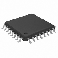
MAX1446EHJ+ Maxim Integrated Products, MAX1446EHJ+ Datasheet - Page 10

MAX1446EHJ+
Manufacturer Part Number
MAX1446EHJ+
Description
IC ADC 10BIT 60MSPS 32-TQFP
Manufacturer
Maxim Integrated Products
Datasheet
1.MAX1446EHJ.pdf
(20 pages)
Specifications of MAX1446EHJ+
Number Of Bits
10
Sampling Rate (per Second)
60M
Data Interface
Parallel
Number Of Converters
1
Voltage Supply Source
Single Supply
Operating Temperature
-40°C ~ 85°C
Mounting Type
Surface Mount
Package / Case
32-TQFP, 32-VQFP
Conversion Rate
60 MSPs
Resolution
10 bit
Snr
59.5 dB
Voltage Reference
2.048 V
Supply Voltage (max)
3.6 V
Supply Voltage (min)
2.7 V
Maximum Power Dissipation
1495.3 mW
Maximum Operating Temperature
+ 85 C
Mounting Style
SMD/SMT
Input Voltage
3 V
Minimum Operating Temperature
- 40 C
Lead Free Status / RoHS Status
Lead free / RoHS Compliant
10-Bit, 60Msps, 3.0V, Low-Power
ADC with Internal Reference
10
4, 5, 8, 11, 14, 30
______________________________________________________________________________________
3, 9, 10
16–20
24–28
PIN
12
13
15
21
22
23
29
31
32
1
2
6
7
REFOUT
D9–D5
D4–D0
NAME
OGND
REFIN
REFN
OV
REFP
COM
GND
V DD
CLK
T.P.
IN+
IN-
PD
OE
DD
Lower Reference. Conversion range is ±(V
capacitor.
Common-Mode Voltage Output. Bypass to GND with a > 0.1µF capacitor.
Analog Supply Voltage. Bypass to GND with a capacitor combination of 2.2µF in parallel
with 0.1µF.
Analog Ground
Positive Analog Input. For single-ended operation, connect signal source to IN+.
Negative Analog Input. For single-ended operation, connect IN- to COM.
Conversion Clock Input
Power-Down Input
High: power-down mode
Low: normal operation
Output Enable Input
High: digital outputs disabled
Low: digital outputs enabled
Three-State Digital Outputs D9–D5. D9 is the MSB.
Output Driver Supply Voltage. Bypass to GND with a capacitor combination of 2.2µF in
parallel with 0.1µF.
Test Point. Do not connect.
Output Driver Ground
Three-State Digital Outputs D4–D0. D0 is the LSB.
Internal Reference Voltage Output. May be connected to REFIN through a resistor or a
resistor-divider.
Reference Input. V
Upper Reference. Conversion range is ±(V
capacitor.
REFIN
= 2 × (V
REFP
- V
FUNCTION
REFN
REFP
REFP
). Bypass to GND with a > 0.01µF capacitor.
- V
- V
REFN
REFN
). Bypass to GND with a > 0.1µF
). Bypass to GND with a > 0.1µF
Pin Description


