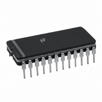
ADC12451CIJ National Semiconductor, ADC12451CIJ Datasheet

ADC12451CIJ
Specifications of ADC12451CIJ
Available stocks
Related parts for ADC12451CIJ
ADC12451CIJ Summary of contents
Page 1
... Bipolar Signal Noise Y Total Harmonic Distortion Y Aperture Time Y Aperture Jitter Y Zero Error Y Positive Full-Scale Error Y Power Consumption Y Connection Diagram Ordering Information ADC12451CIJ TL H 11025 – 1 ADC12451CMJ ADC12451CMJ 883 December 1994 5V reference a 12 bits plus sign (max) 83 kHz (max (min (max) b 100 ns 100 ps rms ...
Page 2
... C V Input Capacitance REF REF C Analog Input Capacitance IN DYNAMIC CHARACTERISTICS Bipolar Effective Bits (Note 17) Unipolar Effective Bits (Note 17 Bipolar Signal to Noise Ratio (Note 17) Operating Ratings (Notes 1 2) Temperature Range ADC12451CIJ ADC12451CMJ ADC12451CMJ 883 and AV Voltage (Notes 3V Negative Supply Voltage (V Reference Voltage ...
Page 3
Converter Electrical Characteristics The following specifications apply for V CC conversion control and MHz unless otherwise specified Boldface limits apply for T e CLK other limits (Notes 6 7 and ...
Page 4
Digital and DC Electrical Characteristics The following specifications apply for DV CC otherwise specified Boldface limits apply for T Symbol Parameter V Logical ‘‘1’’ Input Voltage for IN(1) All Inputs except CLK IN V Logical ‘‘0’’ Input Voltage for IN(0) ...
Page 5
AC Electrical Characteristics The following specifications apply for DV CC Boldface limits apply for MIN Symbol Parameter t Acquisition Time A (Note 15) t Internal Acquisition Time IA (when using WR Control Only) ...
Page 6
Electrical Characteristics (Continued) Note 7 A diode exists between AV and DV as shown below guarantee accuracy it is required that the AV and DV CC Note 8 Accuracy is guaranteed MHz At ...
Page 7
Electrical Characteristics (Continued) FIGURE 1b Simplified Error Curve vs Output Code without Auto-Cal or Auto-Zero Cycles FIGURE 1c Simplified Error Curve vs Output Code after Auto-Cal Cycle Typical Performance Characteristics Zero Error Change vs Ambient Temperature Zero Error vs V ...
Page 8
Typical Performance Characteristics Linearity Error vs Clock Frequency Bipolar Signal-to- Noise Distortion Ratio vs a Input Frequency Bipolar Signal-to- Noise Distortion Ratio vs a Input Signal Level Bipolar Spectral Response with 20 kHz Sine Wave Input (Continued) Bipolar Signal-to- Full ...
Page 9
Typical Performance Characteristics Unipolar Spectral Response with 10 kHz Sine Wave Input Test Circuits FIGURE 2 TRI-STATE Test Circuits and Waveforms (Continued) Unipolar Spectral Response with 20 kHz Sine Wave Input TL H 11025 – 11025 – ...
Page 10
Timing Diagrams Using WR Control to Start a Conversion with Auto-Zero (CAL Auto-Cal Cycle 11025 – 11025 – 17 ...
Page 11
Timing Diagrams (Continued) Using WR Control to Start a Conversion without Auto-Zero (CAL 1 AZ Using S H Control to Start a Conversion without Auto-Zero ( CAL 11025– ...
Page 12
Pin Descriptions DV (24) CC The digital and analog positive power supply AV (4) pins The digital and analog power supply CC voltage range of the ADC12451 guarantee accuracy it is required a that ...
Page 13
Functional Description A conversion sequence can also be controlled by the S H and CS inputs Taking CS and S H low starts the acquisition window for the analog input voltage The rising edge immediately ...
Page 14
Analog Considerations FIGURE 4a Low Drift Extremely Stable Reference Circuit In a ratiometric system the analog input voltage is propor- tional to the voltage used for the A D reference When this voltage is the system power supply ...
Page 15
Analog Considerations 3 5 INPUT BYPASS CAPACITORS An external capacitor can be used to filter out any noise due to inductive pickup by a long input lead and will not degrade the accuracy of the conversion result 3 ...
Page 16
Dynamic Performance Effective number of bits can also be useful in describing the A D’s noise performance An ideal A D converter will have some amount of quantization noise determined by its reso- lution which will yield an ...
Page 17
17 ...
Page 18
... Physical Dimensions inches (millimeters) Order Number ADC12451CMJ ADC12451CMJ 883 or ADC12451CIJ LIFE SUPPORT POLICY NATIONAL’S PRODUCTS ARE NOT AUTHORIZED FOR USE AS CRITICAL COMPONENTS IN LIFE SUPPORT DEVICES OR SYSTEMS WITHOUT THE EXPRESS WRITTEN APPROVAL OF THE PRESIDENT OF NATIONAL SEMICONDUCTOR CORPORATION As used herein 1 Life support devices or systems are devices or ...


