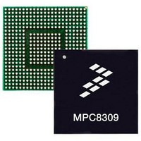
MPC8309VMAHFCA Freescale Semiconductor, MPC8309VMAHFCA Datasheet - Page 10

MPC8309VMAHFCA
Manufacturer Part Number
MPC8309VMAHFCA
Description
417/333/233 MP Std Tmp
Manufacturer
Freescale Semiconductor
Datasheet
1.MPC8309VMAHFCA.pdf
(81 pages)
Specifications of MPC8309VMAHFCA
Processor Series
MPC8309
Core
e300c3
Data Bus Width
32 bit
Data Ram Size
512 MB
Interface Type
USB, CAN, UART, PCI
Maximum Clock Frequency
417 MHz
Number Of Programmable I/os
56
Operating Supply Voltage
- 0.3 V to + 1.26 V
Maximum Operating Temperature
+ 105 C
Mounting Style
SMD/SMT
Operating Temperature Range
0 C to + 105 C
Processor To Be Evaluated
MPC8309
Supply Current (max)
5 uA
Lead Free Status / Rohs Status
Details
Available stocks
Company
Part Number
Manufacturer
Quantity
Price
Company:
Part Number:
MPC8309VMAHFCA
Manufacturer:
Freescale Semiconductor
Quantity:
10 000
Electrical Characteristics
2.1.3
The following table provides information on the characteristics of the output driver strengths.
2.1.4
The following table describes the input capacitance for the SYS_CLK_IN pin in the MPC8309.
2.2
The device does not require the core supply voltage (V
be applied in any particular order. Note that during power ramp-up, before the power supplies are stable
and if the I/O voltages are supplied before the core voltage, there might be a period of time that all input
and output pins are actively driven and cause contention and excessive current. In order to avoid actively
driving the I/O pins and to eliminate excessive current draw, apply the core voltage (V
voltage (GV
where the core voltage is applied first, the core voltage supply must rise to 90% of its nominal value before
the I/O supplies reach 0.7 V; see
stable, wait for a minimum of 32 clock cycles before negating PORESET.
10
Input capacitance for all pins except SYS_CLK_IN and
QE_CLK_IN
Input capacitance for SYS_CLK_IN and QE_CLK_IN
Note:
1. The external clock generator should be able to drive 10 pF.
Local bus interface utilities signals
PCI Signal
DDR2 signal
DUART, system control, I2C, SPI, JTAG
GPIO signals
MPC8309 PowerQUICC II Pro Integrated Communications Processor Family Hardware Specifications, Rev. 1
Power Sequencing
Output Driver Characteristics
Input Capacitance Specification
DD
There is no specific power down sequence requirement for the device. I/O
voltage supplies (GV
with respect to one another.
and OV
Parameter/Condition
Driver Type
DD
) and assert PORESET before the power supplies fully ramp up. In the case
Figure
Table 4. Input Capacitance Specification
DD
Table 3. Output Drive Capability
3. Once both the power supplies (I/O voltage and core voltage) are
and OV
DD
NOTE
) do not have any ordering requirements
C
Symbol
DD
ICLK_IN
Output Impedance
C
I
) and IO supply voltages (GV
()
42
18
42
25
42
Min
10
6
Max
—
8
Freescale Semiconductor
Supply Voltage (V)
DD
DD
OV
GV
OV
OV
) before the I/O
Unit
DD
DD
DD
DD
pF
pF
and OV
= 3.3
= 1.8
= 3.3
= 3.3
DD
Note
—
1
) to


