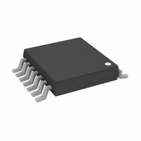
AD5625BRUZ Analog Devices Inc, AD5625BRUZ Datasheet - Page 11

AD5625BRUZ
Manufacturer Part Number
AD5625BRUZ
Description
IC DAC NANO 12BIT QUAD 14-TSSOP
Manufacturer
Analog Devices Inc
Series
nanoDAC™r
Specifications of AD5625BRUZ
Data Interface
I²C, Serial
Settling Time
3µs
Number Of Bits
12
Number Of Converters
4
Voltage Supply Source
Single Supply
Operating Temperature
-40°C ~ 105°C
Mounting Type
Surface Mount
Package / Case
14-TSSOP
Resolution (bits)
12bit
Sampling Rate
333kSPS
Input Channel Type
Serial
Supply Voltage Range - Analogue
2.7V To 5.5V
Supply Current
1.9mA
Digital Ic Case Style
TSSOP
No.
RoHS Compliant
Number Of Channels
4
Resolution
12b
Conversion Rate
333KSPS
Interface Type
Serial (2-Wire/I2C)
Single Supply Voltage (typ)
3.3/5V
Dual Supply Voltage (typ)
Not RequiredV
Architecture
Resistor-String
Power Supply Requirement
Single
Output Type
Voltage
Single Supply Voltage (min)
2.7V
Single Supply Voltage (max)
5.5V
Dual Supply Voltage (min)
Not RequiredV
Dual Supply Voltage (max)
Not RequiredV
Operating Temp Range
-40C to 105C
Operating Temperature Classification
Industrial
Mounting
Surface Mount
Pin Count
14
Lead Free Status / RoHS Status
Lead free / RoHS Compliant
Power Dissipation (max)
-
Lead Free Status / Rohs Status
Compliant
PIN CONFIGURATIONS AND FUNCTION DESCRIPTIONS
Table 7. Pin Function Descriptions
14-Lead
1
2
3
4
5
6
7
8
9
10
11
12
13
14
N/A
Pin Number
Figure 4. Pin Configuration (14-Lead TSSOP), R Suffix Version
10
N/A
3
10-Lead
N/A
N/A
9
1
4
N/A
N/A
5
2
8
7
6
EPAD
V
REFIN
Figure 5. Pin Configuration (14-Lead TSSOP)
ADDR1
V
V
V
LDAC
OUT
OUT
REFIN
/V
POR
V
ADDR1
REFOUT
DD
V
V
LDAC
A
C
OUT
OUT
POR
V
DD
1
2
3
4
5
6
7
Mnemonic
LDAC
ADDR1
V
V
V
POR
V
ADDR2
CLR
V
V
GND
SDA
SCL
ADDR
A
C
DD
OUT
OUT
REFIN
OUT
OUT
1
2
3
4
5
6
7
(Not to Scale)
AD5625/
A
C
D
B
AD5665
TOP VIEW
/V
(Not to Scale)
AD5625R/
AD5645R/
AD5665R
REFOUT
TOP VIEW
Description
Pulsing this pin low allows any or all DAC registers to be updated if the input registers have new data.
This allows simultaneous update of all DAC outputs. Alternatively, this pin can be tied permanently
low.
Three-State Address Input. Sets the two least significant bits (Bit A1, Bit A0) of the 7-bit slave address
(see Table 9).
Power Supply Input. These parts can be operated from 2.7 V to 5.5 V, and the supply should be
decoupled with a 10 μF capacitor in parallel with a 0.1 μF capacitor to GND.
Analog Output Voltage from DAC A. The output amplifier has rail-to-rail operation.
Analog Output Voltage from DAC C. The output amplifier has rail-to-rail operation.
Power-On Reset Pin. Tying the POR pin to GND powers up the part to 0 V. Tying the POR pin to V
powers up the part to midscale.
The AD56x5R have a common pin for reference input and reference output. When using the internal
reference, this is the reference output pin. When using an external reference, this is the reference
input pin. The default for this pin is as a reference input. (The internal reference and reference output
are only available on R suffix versions.) The AD56x5 has a reference input pin only.
Three-State Address Input. Sets Bit A3 and Bit A2 of the 7-bit slave address (see Table 9).
Asynchronous Clear Input. The CLR input is falling-edge sensitive. While CLR is low, all LDAC pulses
are ignored. When CLR is activated, zero scale is loaded to all input and DAC registers. This clears the
output to 0 V. The part exits clear code mode on the falling edge of the ninth clock pulse of the last
byte of the valid write. If CLR is activated during a write sequence, the write is aborted. If CLR is
activated during high speed mode, the part exits high speed mode.
Analog Output Voltage from DAC D. The output amplifier has rail-to-rail operation.
Analog Output Voltage from DAC B. The output amplifier has rail-to-rail operation.
Ground Reference Point for All Circuitry on the Part.
Serial Data Line. This is used in conjunction with the SCL line to clock data into or out of the 16-bit
input register. It is a bidirectional, open-drain data line that should be pulled to the supply with an
external pull-up resistor.
Serial Clock Line. This is used in conjunction with the SDA line to clock data into or out of the 16-bit
input register.
Three-State Address Input. Sets the two least significant bits (Bit A1, Bit A0) of the 7-bit slave address
(see Table 8).
For the 10-lead LFCSP, the exposed pad must be tied to GND.
14
13
12
11
10
9
8
SCL
SDA
GND
V
V
CLR
ADDR2
14
13
12
11
10
9
8
OUT
OUT
SCL
SDA
GND
V
V
CLR
ADDR2
B
D
OUT
OUT
B
D
Rev. B | Page 11 of 36
AD5625R/AD5645R/AD5665R, AD5625/AD5665
Figure 6. Pin Configuration (10-Lead LFCSP), R Suffix Version
V
V
V
V
OUT
OUT
OUT
OUT
Figure 7. Pin Configuration (10-Lead LFCSP)
GND
V
V
V
V
A
B
C
D
EXPOSED PAD TIED TO GND.
OUT
OUT
OUT
OUT
GND
1
2
3
4
5
A
B
C
D
EXPOSED PAD TIED TO GND.
(Not to Scale)
AD5625R/
AD5645R/
1
2
3
4
5
AD5665R
TOP VIEW
(Not to Scale)
AD5625/
AD5665
TOP VIEW
10
9
8
7
6
V
V
SDA
SCL
ADDR
10
REFIN
DD
9
8
7
6
V
V
SDA
SCL
ADDR
REFIN
DD
/V
REFOUT
DD


