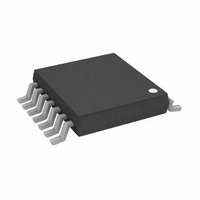
AD5625BRUZ Analog Devices Inc, AD5625BRUZ Datasheet - Page 27

AD5625BRUZ
Manufacturer Part Number
AD5625BRUZ
Description
IC DAC NANO 12BIT QUAD 14-TSSOP
Manufacturer
Analog Devices Inc
Series
nanoDAC™r
Specifications of AD5625BRUZ
Data Interface
I²C, Serial
Settling Time
3µs
Number Of Bits
12
Number Of Converters
4
Voltage Supply Source
Single Supply
Operating Temperature
-40°C ~ 105°C
Mounting Type
Surface Mount
Package / Case
14-TSSOP
Resolution (bits)
12bit
Sampling Rate
333kSPS
Input Channel Type
Serial
Supply Voltage Range - Analogue
2.7V To 5.5V
Supply Current
1.9mA
Digital Ic Case Style
TSSOP
No.
RoHS Compliant
Number Of Channels
4
Resolution
12b
Conversion Rate
333KSPS
Interface Type
Serial (2-Wire/I2C)
Single Supply Voltage (typ)
3.3/5V
Dual Supply Voltage (typ)
Not RequiredV
Architecture
Resistor-String
Power Supply Requirement
Single
Output Type
Voltage
Single Supply Voltage (min)
2.7V
Single Supply Voltage (max)
5.5V
Dual Supply Voltage (min)
Not RequiredV
Dual Supply Voltage (max)
Not RequiredV
Operating Temp Range
-40C to 105C
Operating Temperature Classification
Industrial
Mounting
Surface Mount
Pin Count
14
Lead Free Status / RoHS Status
Lead free / RoHS Compliant
Power Dissipation (max)
-
Lead Free Status / Rohs Status
Compliant
BROADCAST MODE
Broadcast addressing is supported on the AD56x5R/AD56x5
in write mode only. Broadcast addressing can be used to synchro-
nously update or power down multiple AD56x5R/AD56x5
devices. When the broadcast address is used, the AD56x5R/
AD56x5 responds regardless of the states of the address pins.
The AD56x5R/AD56x5 broadcast address is 00010000.
Table 10. Command Definition
C2
0
0
0
0
1
1
1
1
Table 11. DAC Address Command
A2
0
0
0
0
1
C1
0
0
1
1
0
0
1
1
C0
0
1
0
1
0
1
0
1
A1
0
0
1
1
1
Command
Write to input Register n
Update DAC Register n
Write to input Register n, update all
(software LDAC)
Write to and update DAC Channel n
Power up/power down
Reset
LDAC register setup
Internal reference setup (on/off )
A0
0
1
0
1
1
DAC A
DAC B
DAC C
DAC D
All DACs
ADDRESS (n)
Rev. B | Page 27 of 36
AD5625R/AD5645R/AD5665R, AD5625/AD5665
LDAC FUNCTION
The AD56x5R/AD56x5 DACs have double-buffered interfaces
consisting of two banks of registers: input registers and DAC
registers. The input registers are connected directly to the input
shift register, and the digital code is transferred to the relevant
input register upon completion of a valid write sequence. The
DAC registers contain the digital code used by the resistor strings.
Access to the DAC registers is controlled by the LDAC pin.
When the LDAC pin is high, the DAC registers are latched
and the input registers can change state without affecting the
contents of the DAC registers. When LDAC is brought low,
however, the DAC registers become transparent and the contents of
the input registers are transferred to them. The double-buffered
interface is useful if the user requires simultaneous updating of
all DAC outputs. The user can write to one of the input registers
individually and then, by bringing LDAC low when writing to
the other DAC input register, all outputs update simultaneously.
These parts each contain an extra feature whereby a DAC register
is not updated unless its input register has been updated since
the last time LDAC was brought low. Normally, when LDAC is
brought low, the DAC registers are filled with the contents of the
input registers. In the case of the AD56x5R/AD56x5, the DAC
register updates only if the input register has changed since the
last time the DAC register was updated, thereby removing
unnecessary digital crosstalk.
The outputs of all DACs can be simultaneously updated, using
the hardware LDAC pin.
.


