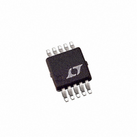
LTC2635CMSE-LMO12#PBF Linear Technology, LTC2635CMSE-LMO12#PBF Datasheet - Page 10

LTC2635CMSE-LMO12#PBF
Manufacturer Part Number
LTC2635CMSE-LMO12#PBF
Description
IC DAC 12BIT I2C QUAD 10MSOP
Manufacturer
Linear Technology
Datasheet
1.LTC2635CMSE-HMI8PBF.pdf
(32 pages)
Specifications of LTC2635CMSE-LMO12#PBF
Settling Time
4.4µs
Number Of Bits
12
Data Interface
I²C
Number Of Converters
4
Voltage Supply Source
Single Supply
Operating Temperature
0°C ~ 70°C
Mounting Type
Surface Mount
Package / Case
10-MSOP Exposed Pad, 10-HMSOP, 10-eMSOP
Lead Free Status / RoHS Status
Lead free / RoHS Compliant
Power Dissipation (max)
-
Available stocks
Company
Part Number
Manufacturer
Quantity
Price
Part Number:
LTC2635CMSE-LMO12#PBFLTC2635CMSE-LMO12#PB
Manufacturer:
LINEAR/凌特
Quantity:
20 000
LTC2635
electrical characteristics
temperature range, otherwise specifications are at T
LTC2635-HMI12/-HMI10/-HMI8/-HZ12/-HZ10/-HZ8 (V
SYMBOL
AC Performance
t
e
timing characteristics
temperature range, otherwise specifications are at T
LTC2635-HMI12/-HMI10/-HMI8/-HZ12/-HZ10/-HZ8 (V
SYMBOL
f
t
t
t
t
t
t
t
t
t
t
t
t
0
S
SCL
HD(STA)
LOW
HIGH
SU(STA)
HD(DAT)
SU(DAT)
r
f
SU(STO)
BUF
1
2
n
PARAMETER
SCL Clock Frequency
Hold Time (Repeated) Start Condition
Low Period of the SCL Clock Pin
High Period of the SCL Clock Pin
Set-Up Time for a Repeated Start Condition
Data Hold Time
Data Set-Up Time
Rise Time of Both SDA and SCL Signals
Fall Time of Both SDA and SCL Signals
Set-Up Time for Stop Condition
Bus Free Time Between a Stop and Start Condition
Falling Edge of 9
High or Low Transition
LDAC Low Pulse Width
PARAMETER
Settling Time
Voltage Output Slew Rate
Capacitive Load Driving
Glitch Impulse
DAC-to-DAC Crosstalk
Multiplying Bandwidth
Output Voltage Noise Density
Output Voltage Noise
th
Clock of the 3
rd
Input Byte to LDAC
A
The
A
FS
FS
CONDITIONS
V
±0.39% (±1LSB at 8 Bits)
±0.098% (±1LSB at 10 Bits)
±0.024% (±1LSB at 12 Bits)
At Mid-Scale Transition
1 DAC Held at FS, 1 DAC Switched 0 to FS
External Reference
At f = 1kHz, External Reference
At f = 10kHz, External Reference
At f = 1kHz, Internal Reference
At f = 10kHz, Internal Reference
0.1Hz to 10Hz, External Reference
0.1Hz to 10Hz, Internal Reference
0.1Hz to 200kHz, External Reference
0.1Hz to 200kHz, Internal Reference
C
CC
REF
= 25°C. V
= 25°C. V
= 4.096V)
= 4.096V)
= 5V (Note 9)
l
= 0.1µF
The
denotes the specifications which apply over the full operating
CONDITIONS
(Note 12)
(Note 12)
l
CC
CC
denotes the specifications which apply over the full operating
= 4.5V to 5.5V, V
= 4.5V to 5.5V. (See Figure 1) (Note 13)
OUT
unloaded unless otherwise specified.
l
l
l
l
l
l
l
l
l
l
l
l
l
20+0.1C
20+0.1C
MIN
MIN
100
400
0.6
1.3
0.6
0.6
0.6
1.3
20
0
0
B
B
TYP
TYP
500
320
180
160
250
230
680
750
3.9
4.3
35
50
5
1
3
3
MAX
MAX
400
300
300
0.9
nV/√Hz
nV/√Hz
nV/√Hz
nV/√Hz
UNITS
UNITS
µV
µV
µV
µV
nV • s
nV • s
2635fb
V/µs
kHz
kHz
P-P
P-P
P-P
P-P
µs
µs
µs
pF
µs
µs
µs
µs
µs
ns
ns
ns
µs
µs
ns
ns


