LTC2655IUF-H12#PBF Linear Technology, LTC2655IUF-H12#PBF Datasheet
LTC2655IUF-H12#PBF
Specifications of LTC2655IUF-H12#PBF
Available stocks


Related parts for LTC2655IUF-H12#PBF


LTC2655IUF-H12#PBF Summary of contents
Page 1
... If PORSEL is tied to GND the DACs power-on reset to zero-scale. If PORSEL is tied to V reset to mid-scale. L, LT, LTC, LTM, Linear Technology and the Linear logo are registered trademarks of Linear Technology Corporation. All other trademarks are the property of their respective owners. Protected by U.S. Patents including 5396245, 6891433 and 7671770. ...
Page 2
LTC2655 ABSOLUTE MAXIMUM RATINGS (Notes 1, 2) Supply Voltage (V ) ................................... –0. SCL, SDA, LDAC, REFLO .............................. –0. ................–0.3V to Min (V OUTA OUTD REFIN/OUT, REFCOMP .....–0.3V to Min (V PORSEL, ...
Page 3
ORDER INFORMATION LTC2655 C UF –L 16 #TR B Consult LTC Marketing for information on non-standard lead based fi nish parts. Consult LTC Marketing for parts specifi ed with wider operating temperature ranges. For more information on lead free part ...
Page 4
... LTC2655IGN-H12#PBF LTC2655IGN-H12#TRPBF LTC2655CUF-H12#PBF LTC2655CUF-H12#TRPBF LTC2655IUF-H12#PBF LTC2655IUF-H12#TRPBF Consult LTC Marketing for parts specifi ed with wider operating temperature ranges. *The temperature grade is identifi label on the shipping container. Consult LTC Marketing for information on non-standard lead based fi nish parts. For more information on lead free part marking, go to: For more information on tape and reel specifi ...
Page 5
ELECTRICAL CHARACTERISTICS temperature range, otherwise specifi cations are at T LTC2655B-L16/ LTC2655-L12 (Internal Reference=1.25V) SYMBOL PARAMETER DC Performance Resolution Monotonicity DNL Differential Nonlinearity INL Integral Nonlinearity (Note 3) Load Regulation ZSE Zero-Scale Error V Offset Error OS V Temperature Coeffi ...
Page 6
LTC2655 ELECTRICAL CHARACTERISTICS temperature range, otherwise specifi cations are at T LTC2655B-L16/LTC2655-L12 (Internal Reference = 1.25V) SYMBOL PARAMETER Reference Reference Output Voltage Reference Temperature Coeffi cient Reference Line Regulation Reference Short-Circuit Current REFCOMP Pin Short-Circuit Current Reference Load Regulation Reference ...
Page 7
ELECTRICAL CHARACTERISTICS temperature range, otherwise specifi cations are at T LTC2655B-H16/LTC2655-H12 (Internal Reference = 2.048V) SYMBOL PARAMETER CONDITIONS DC Performance Resolution Monotonicity (Note 3) DNL Differential Nonlinearity (Note 3) INL Integral Nonlinearity (Note 3) V Load Regulation V Mid-Scale, –15mA ...
Page 8
LTC2655 ELECTRICAL CHARACTERISTICS temperature range, otherwise specifi cations are at T LTC2655B-H16/LTC2655-H12 (Internal Reference = 2.048V) SYMBOL PARAMETER Reference Reference Output Voltage Reference Temperature Coeffi cient Reference Line Regulation Reference Short-Circuit Current REFCOMP Pin Short-Circuit Current Reference Load Regulation Reference ...
Page 9
ELECTRICAL CHARACTERISTICS temperature range, otherwise specifi cations are at T (LTC2655B-H16, LTC2655-H12), V unloaded unless otherwise specifi ed. OUT LTC2655B-L16/LTC2655-L12/LTC2655B-H16/LTC2655-H12 SYMBOL PARAMETER AC Performance t Settling Time ( Note 10) s Settling Time for 1LSB Step Voltage Output Slew Rate ...
Page 10
LTC2655 ELECTRICAL CHARACTERISTICS Note 1: Stresses beyond those listed under Absolute Maximum Ratings may cause permanent damage to the device. Exposure to any Absolute Maximum Rating condition for extended periods may affect device reliability and lifetime. Note 2: All voltages ...
Page 11
TYPICAL PERFORMANCE CHARACTERISTICS LTC2655-L16 Integral Nonlinearity (INL –1 –2 –3 –4 128 16384 32768 CODE INL vs Temperature INL(POS –1 INL(NEG) –2 ...
Page 12
LTC2655 TYPICAL PERFORMANCE CHARACTERISTICS LTC2655-H16 Integral Nonlinearity (INL –1 –2 –3 –4 128 16384 32768 CODE INL vs Temperature INL(POS –1 –2 ...
Page 13
TYPICAL PERFORMANCE CHARACTERISTICS LTC2655-12 Integral Nonlinearity (INL) 1 2.048V REF 0.5 0 –0.5 –1.0 8 1024 2048 3072 CODE 2655 G15 LTC2655 Load Regulation 10 INTERNAL REF 8 CODE = MID-SCALE ...
Page 14
LTC2655 TYPICAL PERFORMANCE CHARACTERISTICS LTC2655 Offset Error vs Reference Input 2 OFFSET ERROR OF 4 CHANNELS 1.5 1.0 0.5 0 –0.5 –1.0 –1.5 –2 0.5 1 1.5 2 REFERENCE VOLTAGE (V) 2655 G24 Supply Current vs ...
Page 15
TYPICAL PERFORMANCE CHARACTERISTICS LTC2655 DAC to DAC Crosstalk (Dynamic) ONE DAC SWITCH 0-FS 1V/DIV V OUT 0.5mV/DIV LTC2655-L16 5V, 0.4nV•s TYP 0.22μF REFCOMP REFOUT 2μs/DIV Power-On Reset to Mid-Scale LTC2655 2V/DIV ...
Page 16
LTC2655 PIN FUNCTIONS (GN/UF) REFLO (Pin 1/Pin 20): Reference Low. The voltage at this pin sets the zero-scale voltage of all DACs. This pin should be tied to GND (Pins 2,4,13,14/Pins 1, 3, 13, 14): DAC OUTA ...
Page 17
BLOCK DIAGRAM REFCOMP GND REFLO V OUTA DAC A V OUTB DAC B CA0 CA1 CA2 SCL LDAC INTERNAL REFERENCE DAC D DAC C POWER-ON RESET 32-BIT SHIFT REGISTER 2-WIRE INTERFACE LTC2655 REFIN/OUT OUTD V OUTC PORSEL ...
Page 18
LTC2655 TEST CIRCUITS TIMING DIAGRAM SDA LOW r SCL t HD(STA HD(DAT) ALL VOLTAGE LEVELS REFER Test Circuit 1 100Ω CAn V /V IH(CA ) IL( 2655 TC01 ...
Page 19
OPERATION The LTC2655 is a family of quad voltage output DACs in 20-lead 4mm × 4mm QFN and in 16-lead narrow SSOP packages. Each DAC can operate rail-to-rail in external reference mode, or with its full-scale voltage set by an ...
Page 20
LTC2655 OPERATION necessary if the bus capacitance is greater than 200pF . The LTC2655 is a receive-only (slave) device. The master can write to the LTC2655. The LTC2655 does not respond to a read command from the master. The START ...
Page 21
OPERATION Write Word Protocol The master initiates communication with the LTC2655 with a START condition and a 7-bit slave address followed by the Write bit ( The LTC2655 acknowledges by pulling the SDA pin low at the 9th ...
Page 22
LTC2655 OPERATION In this case, the power-up delay time is approximately 14μs. The power-up of the integrated reference depends on the command that powered it down. If the reference is powered down using the Select External Reference com- mand (0111b), ...
Page 23
OPERATION Board Layout The excellent load regulation and DC crosstalk performance of these devices is achieved in part by keeping signal and power grounds separate. The PC board should have separate areas for the analog and digital sections of the ...
Page 24
LTC2655 OPERATION 24 2655f ...
Page 25
OPERATION OUTPUT VOLTAGE 0V NEGATIVE INPUT CODE OFFSET (b) Figure 3. Effects of Rail-to-Rail Operation On a DAC Transfer Curve. (a) Overall Transfer Function, (b) Effect of Negative Offset for Codes Near Zero-Scale, (c) Effect of Positive Full-Scale Error for ...
Page 26
LTC2655 PACKAGE DESCRIPTION .254 MIN .0165 ± .0015 RECOMMENDED SOLDER PAD LAYOUT .007 – .0098 (0.178 – 0.249) .016 – .050 (0.406 – 1.270) NOTE: 1. CONTROLLING DIMENSION: INCHES INCHES 2. DIMENSIONS ARE IN (MILLIMETERS) 3. DRAWING NOT TO SCALE ...
Page 27
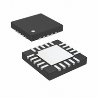
... ON THE TOP AND BOTTOM OF PACKAGE Information furnished by Linear Technology Corporation is believed to be accurate and reliable. However, no responsibility is assumed for its use. Linear Technology Corporation makes no representa- tion that the interconnection of its circuits as described herein will not infringe on existing patent rights. UF Package 20-Lead (4mm × ...
Page 28
... TYPICAL APPLICATION C2 0.1μF +5V C1 0.1μ LDAC V REFCOMP REFIN/OUT CC 7 SCL 9 SDA TO 11 CA0 LTC2655IUF-L16* MICROCONTROLLER 10 CA1 6 CA2 GND GND REFLO *PIN NUMBERS SHOWN ARE FOR THE QFN PACKAGE. RELATED PARTS PART NUMBER DESCRIPTION 2 LTC2609/LTC2619/ Quad 16-/14-/12-Bit LTC2629 2 LTC2605/LTC2615/ ...