LTC2655IUF-H12#PBF Linear Technology, LTC2655IUF-H12#PBF Datasheet - Page 10
LTC2655IUF-H12#PBF
Manufacturer Part Number
LTC2655IUF-H12#PBF
Description
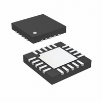
IC DAC 12BIT QUAD CUR OUT 20QFN
Manufacturer
Linear Technology
Datasheet
1.LTC2655CGN-H12PBF.pdf
(28 pages)
Specifications of LTC2655IUF-H12#PBF
Settling Time
3.9µs
Number Of Bits
12
Data Interface
I²C, Serial
Number Of Converters
4
Voltage Supply Source
Single Supply
Operating Temperature
-40°C ~ 85°C
Mounting Type
Surface Mount
Package / Case
20-WQFN Exposed Pad, 20-DQFN
Lead Free Status / RoHS Status
Lead free / RoHS Compliant
Power Dissipation (max)
-
Available stocks
Company
Part Number
Manufacturer
Quantity
Price


LTC2655
ELECTRICAL CHARACTERISTICS
Note 1: Stresses beyond those listed under Absolute Maximum Ratings
may cause permanent damage to the device. Exposure to any Absolute
Maximum Rating condition for extended periods may affect device
reliability and lifetime.
Note 2: All voltages are with respect to GND.
Note 3: Linearity and monotonicity are defi ned from code k
where N is the resolution and k
limiting occurs. For V
defi ned from code 128 to code 65535. For V
and linearity is defi ned from code 8 to code 4095.
Note 4: Inferred from measurement at code 128 (LTC2655-16), or code 8
(LTC2655-12).
Note 5: DC Crosstalk is measured with V
reference, with the measured DAC at mid-scale.
Note 6: This IC includes current limiting that is intended to protect the
device during momentary overload conditions. Junction temperature can
exceed the rated maximum during current limiting. Continuous operation
above the specifi ed maximum operating junction temperature may impair
device reliability.
10
REF
= 2.5V and N = 16, k
L
is the lower end code for which no output
CC
= 5V and using internal
REF
L
= 128 and linearity is
= 2.5V and N = 12, k
L
to code 2
L
N
=8
–1,
Note 7: Temperature coeffi cient is calculated by dividing the maximum
change in output voltage by the specifi ed temperature range. Maximum
temperature coeffi cient is guaranteed for C-grade only.
Note 8: Digital inputs at 0V or V
Note 9: Guaranteed by design and not production tested.
Note 10: Internal Reference mode. DAC is stepped 1/4 scale to 3/4 scale
and 3/4 scale to 1/4 scale. Load is 2kΩ in parallel with 200pF to GND.
Note 11: V
reference mode. DAC is stepped ±1 LSB between half-scale and
half-scale – 1. Load is 2kΩ n parallel with 200pF to GND.
Note 12: DAC to DAC Crosstalk is the glitch that appears at the output
of one DAC due to a full scale change at the output of another DAC. It is
measured with V
DAC at mid-scale.
Note 13: C
Note 14: Gain error specifi cation may be degraded for reference input
voltages less than 1V. See Gain Error vs Reference Input Curve in the
Typical Performance Characteristics section.
CC
B
= Capacitance of one bus line in pF .
= 5V (-H Options) or V
CC
= 5V and using internal reference, with the measured
CC
.
CC
= 3V (-L Options), internal
2655f
Related parts for LTC2655IUF-H12#PBF
Image
Part Number
Description
Manufacturer
Datasheet
Request
R

Part Number:
Description:
IC DAC 12BIT QUAD CUR OUT 20QFN
Manufacturer:
Linear Technology
Datasheet:
Part Number:
Description:
IC DAC 12BIT QUAD CUR OUT 20QFN
Manufacturer:
Linear Technology
Datasheet:
Part Number:
Description:
IC DAC 12BIT QUAD CUR OUT 20QFN
Manufacturer:
Linear Technology
Datasheet:

Part Number:
Description:
CD ROM LINEARVIEW DATASHEETS
Manufacturer:
Linear Technology

Part Number:
Description:
Standalone Linear Li-Ion Battery Charger with Thermal Regulation in ThinSOT
Manufacturer:
Linear Technology Corporation
Datasheet:
Part Number:
Description:
Low noise, high frequency, 8th order linear phase lowpass filter
Manufacturer:
Linear Technology Corporation
Datasheet:
Part Number:
Description:
Manufacturer:
Linear Technology Corporation
Datasheet:
Part Number:
Description:
Manufacturer:
Linear Technology Corporation
Datasheet:
Part Number:
Description:
Manufacturer:
Linear Technology Corporation
Datasheet:
Part Number:
Description:
Manufacturer:
Linear Technology Corporation
Datasheet:
Part Number:
Description:
Manufacturer:
Linear Technology Corporation
Datasheet:
Part Number:
Description:
Manufacturer:
Linear Technology Corporation
Datasheet:
Part Number:
Description:
Manufacturer:
Linear Technology Corporation
Datasheet:
Part Number:
Description:
Dual and Quad, JFET Input Precision High Speed Op Amps
Manufacturer:
Linear Technology Corporation
Datasheet:
Part Number:
Description:
Manufacturer:
Linear Technology Corporation
Datasheet: