LTC2754IUKG-12#TRPBF Linear Technology, LTC2754IUKG-12#TRPBF Datasheet - Page 22
LTC2754IUKG-12#TRPBF
Manufacturer Part Number
LTC2754IUKG-12#TRPBF
Description
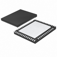
IC DAC 12BIT QUAD IOUT 52-QFN
Manufacturer
Linear Technology
Datasheet
1.LTC2754IUKG-12PBF.pdf
(28 pages)
Specifications of LTC2754IUKG-12#TRPBF
Settling Time
2µs
Number Of Bits
12
Data Interface
Serial, SPI™
Number Of Converters
4
Voltage Supply Source
Single Supply
Operating Temperature
-40°C ~ 85°C
Mounting Type
Surface Mount
Package / Case
52-QFN
Lead Free Status / RoHS Status
Lead free / RoHS Compliant
Power Dissipation (max)
-
Available stocks
Company
Part Number
Manufacturer
Quantity
Price

Part Number:
LTC2754IUKG-12#TRPBFLTC2754IUKG-12#PBF
Manufacturer:
Linear Technology
Quantity:
135


LTC2754
APPLICATIONS INFORMATION
As precision DAC applications move to 16-bit and higher
performance, reference output voltage noise may contrib-
ute a dominant share of the system’s noise fl oor. This in
turn can degrade system dynamic range and signal-to-
noise ratio. Care should be exercised in selecting a voltage
reference with as low an output noise voltage as practi-
cal for the system resolution desired. Precision voltage
references, like the LT1236, produce low output noise in
the 0.1Hz to 10Hz region, well below the 16-bit LSB level
in 5V or 10V full-scale systems. However, as the circuit
bandwidths increase, fi ltering the output of the reference
may be required to minimize output noise.
Grounding
As with any high resolution converter, clean grounding is
important. A low impedance analog ground plane and star
grounding techniques should be used. I
to the star ground with as low a resistance as possible.
22
OUT2X
must be tied
When it is not possible to locate star ground close to
I
pin to star ground. This minimizes the voltage drop from
this pin to ground caused by the code-dependent current
fl owing to ground. When the resistance of this circuit
board trace becomes greater than 1Ω, a force/sense am-
plifi er confi guration should be used to drive this pin (see
Figure 5). This preserves the excellent accuracy (1LSB
INL and DNL) of the LTC2754-16.
Layout
Figures 6, 7, 8, and 9 show the layout for the LTC2754
evaluation board, DC1546. This shows how to route the
digital signals around the device without interfering with
the reference and output op amps. Complete demo board
documentation is available in the DC1546 “Quick Start
Guide.”
OUT2
, a low resistance trace should be used to route this
2754f
Related parts for LTC2754IUKG-12#TRPBF
Image
Part Number
Description
Manufacturer
Datasheet
Request
R

Part Number:
Description:
IC DAC 12BIT QUAD IOUT 52-QFN
Manufacturer:
Linear Technology
Datasheet:

Part Number:
Description:
CD ROM LINEARVIEW DATASHEETS
Manufacturer:
Linear Technology

Part Number:
Description:
Standalone Linear Li-Ion Battery Charger with Thermal Regulation in ThinSOT
Manufacturer:
Linear Technology Corporation
Datasheet:
Part Number:
Description:
Low noise, high frequency, 8th order linear phase lowpass filter
Manufacturer:
Linear Technology Corporation
Datasheet:
Part Number:
Description:
Manufacturer:
Linear Technology Corporation
Datasheet:
Part Number:
Description:
Manufacturer:
Linear Technology Corporation
Datasheet:
Part Number:
Description:
Manufacturer:
Linear Technology Corporation
Datasheet:
Part Number:
Description:
Manufacturer:
Linear Technology Corporation
Datasheet:
Part Number:
Description:
Manufacturer:
Linear Technology Corporation
Datasheet:
Part Number:
Description:
Manufacturer:
Linear Technology Corporation
Datasheet:
Part Number:
Description:
Manufacturer:
Linear Technology Corporation
Datasheet:
Part Number:
Description:
Dual and Quad, JFET Input Precision High Speed Op Amps
Manufacturer:
Linear Technology Corporation
Datasheet:
Part Number:
Description:
Manufacturer:
Linear Technology Corporation
Datasheet:
Part Number:
Description:
1, 2, 6 and 8 Channel, 10-Bit Serial I/O Data Acquisition Systems
Manufacturer:
Linear Technology Corporation
Datasheet:
Part Number:
Description:
Manufacturer:
Linear Technology Corporation
Datasheet: