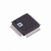
AD9751AST Analog Devices Inc, AD9751AST Datasheet - Page 11

AD9751AST
Manufacturer Part Number
AD9751AST
Description
IC DAC 10BIT 300MSPS 48-LQFP
Manufacturer
Analog Devices Inc
Series
TxDAC+®r
Datasheet
1.AD9751ASTZ.pdf
(28 pages)
Specifications of AD9751AST
Rohs Status
RoHS non-compliant
Settling Time
11ns
Number Of Bits
10
Data Interface
Parallel
Number Of Converters
1
Voltage Supply Source
Analog and Digital
Power Dissipation (max)
165mW
Operating Temperature
-40°C ~ 85°C
Mounting Type
Surface Mount
Package / Case
48-LQFP
For Use With
AD9751-EB - BOARD EVAL FOR AD9751
Available stocks
Company
Part Number
Manufacturer
Quantity
Price
Company:
Part Number:
AD9751AST
Manufacturer:
AD
Quantity:
1 831
Company:
Part Number:
AD9751AST
Manufacturer:
ADI
Quantity:
455
Part Number:
AD9751AST
Manufacturer:
ADI/亚德诺
Quantity:
20 000
Company:
Part Number:
AD9751ASTZ
Manufacturer:
Analog Devices Inc
Quantity:
10 000
Part Number:
AD9751ASTZ
Manufacturer:
ADI/亚德诺
Quantity:
20 000
Company:
Part Number:
AD9751ASTZRL
Manufacturer:
Analog Devices Inc
Quantity:
10 000
PLL CLOCK MULTIPLIER OPERATION
The Phase-Locked Loop (PLL) is intrinsic to the operation of the
AD9751 in that it produces the necessary internally synchronized
2× clock for the edge-triggered latches, multiplexer, and DAC.
With PLLVDD connected to its supply voltage, the AD9751 is
in PLL active mode. Figure 6 shows a functional block diagram
of the AD9751 clock control circuitry with PLL active. The
circuitry consists of a phase detector, charge pump, voltage
controlled oscillator (VCO), input data rate range control, clock
logic circuitry, and control input/outputs. The ÷ 2 logic in the
feedback loop allows the PLL to generate the 2× clock needed
for the DAC output latch.
Figure 7 defines the input and output timing for the AD9751
with the PLL active. CLK in Figure 7 represents the clock that
is generated external to the AD9751. The input data at both
Ports 1 and 2 is latched on the same CLK rising edge. CLK
may be applied as a single-ended signal by tying CLK– to
midsupply and applying CLK to CLK+, or as a differential
signal applied to CLK+ and CLK–.
RESET has no purpose when using the internal PLL and
should be grounded. When the AD9751 is in PLL active
mode, PLLLOCK is the output of the internal phase detector.
When locked, the lock output in this mode is Logic 1.
REV. C
CLK+
CLK–
ADDITIONAL
EXTERNAL
SINGLE-ENDED
DIFFERENTIAL
Figure 5. External Reference Configuration
LOAD
Figure 4. Internal Reference Configuration
REFERENCE
Figure 6. Clock Circuitry with PLL Active
EXTERNAL
REFERENCE
AMP
EXTERNAL
OPTIONAL
TO
AVDD
BUFFER
(3.0V TO 3.6V)
AD9751
I
CLKVDD
REF
TO INPUT
LATCHES
DETECTOR
I
PHASE
0.1 F
REF
2k
PLLLOCK
REFIO
FSADJ
2k
1.2V REF
REFIO
FSADJ
REFERENCE
CHARGE
AD9751
SECTION
PUMP
1.2V REF
TO DAC
LATCH
2
REFERENCE
LPF
AD9751
SECTION
( 1, 2, 4, 8)
392
CONTROL
CLKCOM
CURRENT
RANGE
SOURCE
ARRAY
VCO
PLLVDD
AVDD
1.0
CURRENT
SOURCE
ARRAY
F
AVDD
DIV0
DIV1
3.0V TO
3.6V
–11–
Typically, the VCO can generate outputs of 100 MHz to 400 MHz.
The range control is used to keep the VCO operating within its
designed range while allowing input clocks as low as 6.25 MHz.
With the PLL active, logic levels at DIV0 and DIV1 determine
the divide (prescaler) ratio of the range controller. Table I gives
the frequency range of the input clock for the different states of
DIV0 and DIV1.
CLK Frequency
50 MHz–150 MHz
25 MHz–100 MHz
12.5 MHz–50 MHz
6.25 MHz–25 MHz
A 392 Ω resistor and 1.0 µF capacitor connected in series from
LPF to PLLVDD are required to optimize the phase noise versus
settling/acquisition time characteristics of the PLL. To obtain
optimum noise and distortion performance, PLLVDD should
be set to a voltage level similar to DVDD and CLKVDD.
In general, the best phase noise performance for any PLL range
control setting is achieved with the VCO operating near its
maximum output frequency of 400 MHz.
As stated earlier, applications requiring input data rates below
6.25 MSPS must disable the PLL clock multiplier and provide an
external 2× reference clock. At higher data rates however, applica-
tions already containing a low phase noise (i.e., jitter) reference
clock that is twice the input data rate should consider disabling the
PLL clock multiplier to achieve the best SNR performance from the
AD9751. Note that the SFDR performance of the AD9751 remains
unaffected with or without the PLL clock multiplier enabled.
Table I. CLK Rates for DIV0, DIV1 Levels with PLL Active
I
OUTA
I
OUTA
OR I
DATA IN
PORT 1
PORT 2
DATA IN
OR I
7a. DAC Input Timing Requirements with
PLL Active, Single Clock Cycle
Figure 7b. DAC Input Timing Requirements with
PLL Active, Multiple Clock Cycles
PORT 1
PORT 2
OUTB
CLK
OUTB
CLK
t
DATA X
DATA Y
S
DATA X
DATA W
DIV1
0
0
1
1
t
t
H
1/2 CYCLE +
LPW
XXX
DATA W
t
DIV0
0
1
0
1
PD
DATA Y
DATA Z
DATA X
DATA X
Range Controller
÷ 1
÷ 2
÷ 4
÷ 8
DATA Y
AD9751
t
PD
DATA Z
DATA Y


