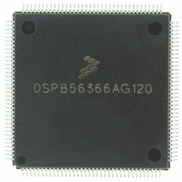
DSPB56366AG120 Freescale Semiconductor, DSPB56366AG120 Datasheet - Page 82

DSPB56366AG120
Manufacturer Part Number
DSPB56366AG120
Description
IC DSP 24BIT AUD 120MHZ 144-LQFP
Manufacturer
Freescale Semiconductor
Series
Symphony™r
Type
Audio Processorr
Datasheet
1.DSPB56366AG120.pdf
(110 pages)
Specifications of DSPB56366AG120
Interface
Host Interface, I²C, SAI, SPI
Clock Rate
120MHz
Non-volatile Memory
ROM (240 kB)
On-chip Ram
69kB
Voltage - I/o
3.30V
Voltage - Core
3.30V
Operating Temperature
-40°C ~ 110°C
Mounting Type
Surface Mount
Package / Case
144-LQFP
Lead Free Status / RoHS Status
Lead free / RoHS Compliant
Available stocks
Company
Part Number
Manufacturer
Quantity
Price
Company:
Part Number:
DSPB56366AG120
Manufacturer:
TOSHIBA
Quantity:
639
Company:
Part Number:
DSPB56366AG120
Manufacturer:
FREESCAL
Quantity:
273
Company:
Part Number:
DSPB56366AG120
Manufacturer:
Freescale Semiconductor
Quantity:
10 000
3-56
1
2
3
4
5
6
7
460
461
462
463
464
465
No.
V
i ck = internal clock
x ck = external clock
i ck a = internal clock, asynchronous mode
(asynchronous implies that TXC and RXC are two different clocks)
i ck s = internal clock, synchronous mode
(synchronous implies that TXC and RXC are the same clock)
bl = bit length
wl = word length
wr = word length relative
TXC(SCKT pin) = transmit clock
RXC(SCKR pin) = receive clock
FST(FST pin) = transmit frame sync
FSR(FSR pin) = receive frame sync
HCKT(HCKT pin) = transmit high frequency clock
HCKR(HCKR pin) = receive high frequency clock
For the internal clock, the external clock cycle is defined by Icyc and the ESAI control register.
The word-relative frame sync signal waveform relative to the clock operates in the same manner as the bit-length frame sync
signal waveform, but spreads from one serial clock before first bit clock (same as bit length frame sync signal), until the one
before last bit clock of the first word in frame.
Periodically sampled and not 100% tested
CC
= 3.16 V ± 0.16 V; T
FST input (wl) setup time before TXC
falling edge
FST input hold time after TXC falling
edge
Flag output valid after TXC rising edge
HCKR/HCKT clock cycle
HCKT input rising edge to TXC output
HCKR input rising edge to RXC output
Characteristics
Table 3-22 Enhanced Serial Audio Interface Timing (continued)
J
= –40°C to +110°C, C
1, 2, 3
DSP56366 Technical Data, Rev. 3.1
L
Symbol
= 50 pF
—
—
—
—
—
—
Expression
—
—
—
—
—
—
21.0
40.0
Min
2.0
4.0
0.0
—
—
—
—
Max
32.0
18.0
27.5
27.5
—
—
—
—
—
Freescale Semiconductor
Condition
x ck
x ck
x ck
i ck
i ck
i ck
4
Unit
ns
ns
ns
ns
ns
ns


