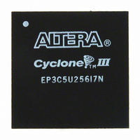
EP3C5U256I7N Altera, EP3C5U256I7N Datasheet - Page 71

EP3C5U256I7N
Manufacturer Part Number
EP3C5U256I7N
Description
IC CYCLONE III FPGA 5K 256 UBGA
Manufacturer
Altera
Series
Cyclone® IIIr
Datasheets
1.EP3C5F256C8N.pdf
(5 pages)
2.EP3C5F256C8N.pdf
(34 pages)
3.EP3C5F256C8N.pdf
(66 pages)
4.EP3C5F256C8N.pdf
(14 pages)
5.EP3C5F256C8N.pdf
(76 pages)
6.EP3C5U256I7N.pdf
(274 pages)
Specifications of EP3C5U256I7N
Number Of Logic Elements/cells
5136
Number Of Labs/clbs
321
Total Ram Bits
423936
Number Of I /o
182
Voltage - Supply
1.15 V ~ 1.25 V
Mounting Type
Surface Mount
Operating Temperature
-40°C ~ 100°C
Package / Case
256-UBGA
Family Name
Cyclone III
Number Of Logic Blocks/elements
5136
# I/os (max)
182
Frequency (max)
437.5MHz
Process Technology
65nm
Operating Supply Voltage (typ)
1.2V
Logic Cells
5136
Ram Bits
423936
Operating Supply Voltage (min)
1.15V
Operating Supply Voltage (max)
1.25V
Operating Temp Range
-40C to 100C
Operating Temperature Classification
Industrial
Mounting
Surface Mount
Pin Count
256
Package Type
UFBGA
For Use With
544-2601 - KIT DEV CYCLONE III LS EP3CLS200544-2411 - KIT DEV NIOS II CYCLONE III ED.
Lead Free Status / RoHS Status
Lead free / RoHS Compliant
Number Of Gates
-
Lead Free Status / Rohs Status
Compliant
Other names
544-2560
Available stocks
Company
Part Number
Manufacturer
Quantity
Price
Company:
Part Number:
EP3C5U256I7N
Manufacturer:
ALTERA21
Quantity:
201
Part Number:
EP3C5U256I7N
Manufacturer:
ALTERA/阿尔特拉
Quantity:
20 000
Chapter 2: Cyclone III LS Device Data Sheet
Glossary
Table 2–39. Glossary (Part 2 of 5)
© December 2009
Letter
Q
R
P
PLL Block
R
Receiver Input
Waveform
RSKM (Receiver
input skew
margin)
L
Term
—
Altera Corporation
The following block diagram highlights the PLL specification parameters.
Receiver differential input discrete resistor (external to the Cyclone III LS device)
Receiver Input Waveform for LVDS and LVPECL Differential Standards
High-speed I/O Block: The total margin left after accounting for the sampling window and
TCCS. RSKM = (TUI – SW – TCCS) / 2
Core Clock
Key
Single-Ended Waveform
Differential Input Waveform
CLK
Reconfigurable in User Mode
V
CM
Switchover
V
f
ID
IN
N
f
INPFD
V
ID
Definitions
PFD
—
M
CP
Phase tap
LF
VCO
Cyclone III Device Handbook, Volume 2
f
VCO
V
p - n
Positive Channel (p) = V
Negative Channel (n) = V
Ground
ID
0 V
Counters
C0..C4
CLKOUT Pins
f
f
OUT _EXT
OUT
GCLK
IH
IL
2–27


