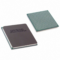
EP3SL150F780C4N Altera, EP3SL150F780C4N Datasheet - Page 320

EP3SL150F780C4N
Manufacturer Part Number
EP3SL150F780C4N
Description
IC STRATIX III FPGA 150K 780FBGA
Manufacturer
Altera
Series
Stratix® IIIr
Datasheets
1.EP3SL150F780C4N.pdf
(16 pages)
2.EP3SL150F780C4N.pdf
(332 pages)
3.EP3SL150F780C4N.pdf
(456 pages)
4.EP3SL150F780C4N.pdf
(341 pages)
Specifications of EP3SL150F780C4N
Number Of Logic Elements/cells
142500
Number Of Labs/clbs
5700
Total Ram Bits
6390
Number Of I /o
488
Voltage - Supply
0.86 V ~ 1.15 V
Mounting Type
Surface Mount
Operating Temperature
0°C ~ 85°C
Package / Case
780-FBGA
Family Name
Stratix III
Number Of Logic Blocks/elements
142500
# I/os (max)
488
Frequency (max)
450MHz
Process Technology
65nm
Operating Supply Voltage (typ)
1.1V
Logic Cells
142500
Ram Bits
6543360
Operating Supply Voltage (min)
1.05V
Operating Supply Voltage (max)
1.15V
Operating Temp Range
0C to 85C
Operating Temperature Classification
Commercial
Mounting
Surface Mount
Pin Count
780
Package Type
FC-FBGA
For Use With
544-2568 - KIT DEVELOPMENT STRATIX III
Lead Free Status / RoHS Status
Lead free / RoHS Compliant
Number Of Gates
-
Lead Free Status / Rohs Status
Compliant
Other names
544-2403
EP3SL150F780C4NES
EP3SL150F780C4NES
Available stocks
Company
Part Number
Manufacturer
Quantity
Price
Company:
Part Number:
EP3SL150F780C4N
Manufacturer:
ALTERA
Quantity:
3 000
- EP3SL150F780C4N PDF datasheet
- EP3SL150F780C4N PDF datasheet #2
- EP3SL150F780C4N PDF datasheet #3
- EP3SL150F780C4N PDF datasheet #4
- Current page: 320 of 341
- Download datasheet (4Mb)
1–310
Dedicated Clock Pin Timing
Table 1–142. EP3SL50 Column Pin Global Clock Timing Specifications
Table 1–143. EP3SL50 Row Pin Global Clock Timing Specifications
Table 1–144. EP3SL50 Column Pin Regional Clock Timing Specifications (Part 1 of 2)
Stratix III Device Handbook, Volume 2
t
t
t
t
t
t
t
t
t
t
Parameter
Parameter
Parameter
CIN
COUT
PLLCIN
PLLCOUT
CIN
COUT
PLLCIN
PLLCOUT
CIN
COUT
Industrial
Industrial
Industrial
-0.034
-0.018
-0.018
1.732
1.650
0.048
1.689
1.689
1.736
1.736
Fast Model
Fast Model
Fast Model
Table 1–141
driven by the global clock, regional clock, periphery clock, and a PLL.
Table 1–141
Table 1–141. Clock Timing Parameters for Stratix III Devices
EP3SL50 Clock Timing Parameters
Table 1–142
devices.
Table 1–144
devices.
t
t
t
t
CIN
COUT
PLLCIN
PLLCOUT
Commercial
Commercial
Commercial
Symbol
-0.026
-0.026
1.843
1.752
0.116
0.025
1.669
1.669
1.737
1.737
to
lists the Stratix III clock timing parameters.
and
and
Table 1–201
Table 1–143
Table 1–145
-0.142 -0.216 -0.181
-0.284 -0.379 -0.362
2.527
2.385
2.371
2.371
-0.261
-0.261
1.1 V
1.1 V
2.436
2.436
V
V
1.1 V
V
Delay from the clock pad to the I/O input register
Delay from the clock pad to the I/O output register
Delay from the PLL inclk pad to the I/O input register
Delay from the PLL inclk pad to the I/O output register
C2
C2
CCL
CCL
C2
CCL
=
=
=
2.758
2.595
2.645
2.645
-0.312
-0.312
1.1 V
1.1 V
V
V
2.691
2.691
list clock pin timing for Stratix III devices when the clock is
1.1 V
V
C3
C3
CCL
CCL
C3
CCL
list the global clock timing parameters for EP3SL50
list the regional clock timing parameters for EP3SL50
=
=
=
Chapter 1: Stratix III Device Datasheet: DC and Switching Characteristics
3.099
2.918
3.004
3.004
1.1 V
1.1 V
-0.251
-0.251
V
V
3.056
3.056
1.1 V
V
C4
C4
CCL
CCL
C4
CCL
=
=
=
-0.136
-0.307
2.997
2.826
2.719
2.719
1.1 V
1.1 V
-0.230
-0.230
V
V
2.925
2.925
1.1 V
V
CCL
CCL
CCL
=
=
=
C4L
C4L
C4L
Parameter
-0.188
-0.347
3.227
3.068
3.136
3.136
0.9 V
0.9 V
V
V
-0.011
-0.011
3.433
3.433
0.9 V
V
CCL
CCL
CCL
=
=
=
-0.173
-0.343
2.811
2.641
2.645
2.645
1.1 V
1.1 V
V
V
-0.312
-0.312
2.691
2.691
1.1 V
V
I3
CCL
I3
CCL
I3
CCL
=
=
=
© July 2010 Altera Corporation
3.146
2.957
0.265
0.076
3.009
3.009
1.1 V
1.1 V
V
V
3.056
3.056
0.161
0.161
1.1 V
I4
CCL
I4
CCL
V
I4
CCL
=
=
=
-0.087 -0.230
-0.266 -0.389
3.055
2.876
2.719
2.719
1.1 V
1.1 V
V
V
-0.230
-0.230
2.925
2.925
1.1 V
CCL
CCL
V
CCL
=
=
=
I4L
I4L
I/O Timing
I4L
3.260
3.101
3.136
3.136
0.9 V
0.9 V
V
V
-0.011
-0.011
3.433
3.433
CCL
CCL
0.9 V
V
CCL
=
=
=
Units
Units
ns
ns
ns
ns
ns
ns
Units
ns
ns
ns
ns
Related parts for EP3SL150F780C4N
Image
Part Number
Description
Manufacturer
Datasheet
Request
R

Part Number:
Description:
CYCLONE II STARTER KIT EP2C20N
Manufacturer:
Altera
Datasheet:

Part Number:
Description:
CPLD, EP610 Family, ECMOS Process, 300 Gates, 16 Macro Cells, 16 Reg., 16 User I/Os, 5V Supply, 35 Speed Grade, 24DIP
Manufacturer:
Altera Corporation
Datasheet:

Part Number:
Description:
CPLD, EP610 Family, ECMOS Process, 300 Gates, 16 Macro Cells, 16 Reg., 16 User I/Os, 5V Supply, 15 Speed Grade, 24DIP
Manufacturer:
Altera Corporation
Datasheet:

Part Number:
Description:
Manufacturer:
Altera Corporation
Datasheet:

Part Number:
Description:
CPLD, EP610 Family, ECMOS Process, 300 Gates, 16 Macro Cells, 16 Reg., 16 User I/Os, 5V Supply, 30 Speed Grade, 24DIP
Manufacturer:
Altera Corporation
Datasheet:

Part Number:
Description:
High-performance, low-power erasable programmable logic devices with 8 macrocells, 10ns
Manufacturer:
Altera Corporation
Datasheet:

Part Number:
Description:
High-performance, low-power erasable programmable logic devices with 8 macrocells, 7ns
Manufacturer:
Altera Corporation
Datasheet:

Part Number:
Description:
Classic EPLD
Manufacturer:
Altera Corporation
Datasheet:

Part Number:
Description:
High-performance, low-power erasable programmable logic devices with 8 macrocells, 10ns
Manufacturer:
Altera Corporation
Datasheet:

Part Number:
Description:
Manufacturer:
Altera Corporation
Datasheet:

Part Number:
Description:
Manufacturer:
Altera Corporation
Datasheet:

Part Number:
Description:
Manufacturer:
Altera Corporation
Datasheet:

Part Number:
Description:
CPLD, EP610 Family, ECMOS Process, 300 Gates, 16 Macro Cells, 16 Reg., 16 User I/Os, 5V Supply, 25 Speed Grade, 24DIP
Manufacturer:
Altera Corporation
Datasheet:


