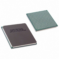
EP3SL150F780C4N Altera, EP3SL150F780C4N Datasheet - Page 144

EP3SL150F780C4N
Manufacturer Part Number
EP3SL150F780C4N
Description
IC STRATIX III FPGA 150K 780FBGA
Manufacturer
Altera
Series
Stratix® IIIr
Datasheets
1.EP3SL150F780C4N.pdf
(16 pages)
2.EP3SL150F780C4N.pdf
(332 pages)
3.EP3SL150F780C4N.pdf
(456 pages)
4.EP3SL150F780C4N.pdf
(341 pages)
Specifications of EP3SL150F780C4N
Number Of Logic Elements/cells
142500
Number Of Labs/clbs
5700
Total Ram Bits
6390
Number Of I /o
488
Voltage - Supply
0.86 V ~ 1.15 V
Mounting Type
Surface Mount
Operating Temperature
0°C ~ 85°C
Package / Case
780-FBGA
Family Name
Stratix III
Number Of Logic Blocks/elements
142500
# I/os (max)
488
Frequency (max)
450MHz
Process Technology
65nm
Operating Supply Voltage (typ)
1.1V
Logic Cells
142500
Ram Bits
6543360
Operating Supply Voltage (min)
1.05V
Operating Supply Voltage (max)
1.15V
Operating Temp Range
0C to 85C
Operating Temperature Classification
Commercial
Mounting
Surface Mount
Pin Count
780
Package Type
FC-FBGA
For Use With
544-2568 - KIT DEVELOPMENT STRATIX III
Lead Free Status / RoHS Status
Lead free / RoHS Compliant
Number Of Gates
-
Lead Free Status / Rohs Status
Compliant
Other names
544-2403
EP3SL150F780C4NES
EP3SL150F780C4NES
Available stocks
Company
Part Number
Manufacturer
Quantity
Price
Company:
Part Number:
EP3SL150F780C4N
Manufacturer:
ALTERA
Quantity:
3 000
- EP3SL150F780C4N PDF datasheet
- EP3SL150F780C4N PDF datasheet #2
- EP3SL150F780C4N PDF datasheet #3
- EP3SL150F780C4N PDF datasheet #4
- Current page: 144 of 456
- Download datasheet (7Mb)
5–38
Figure 5–23. FIR Filter using Tap-Delay Line Input and Chained Cascade Summation of Final Result
Stratix III Device Handbook, Volume 1
datab_0[17..0]
datab_1[17..0]
datab_2[17..0]
datab_3[17..0]
datab_4[17..0]
datab_5[17..0]
datab_6[17..0]
datab_7[17..0]
dataa_0[ ]
In
Four-Multiplier Adder is shown as the chainout adder for clarity. This scheme is used
to chain and add multiple DSP blocks together. The output of the chainout adder can
be registered. The registered chainout output can feed the lower adjacent DSP block
for a chainout summation or it can feed general FPGA routing. The chainout result
can be zeroed out by applying logic 1 on the dynamic zerochainout signal. The
zerochainout signal can also be registered.
Delay Register
Figure
clock[3..0]
ena[3..0]
aclr[3..0]
5–23, the adder that adds the adjacent half DSP block to the current
+
+
+
+
chainout_saturate
chainout_round
zero_chainout
signa
signb
+
+
Half-DSP Block
Half-DSP Block
Zero
+
+
chainout_sat_overflow
Chapter 5: DSP Blocks in Stratix III Devices
© March 2010 Altera Corporation
44
result[ ]
Application Examples
Related parts for EP3SL150F780C4N
Image
Part Number
Description
Manufacturer
Datasheet
Request
R

Part Number:
Description:
CYCLONE II STARTER KIT EP2C20N
Manufacturer:
Altera
Datasheet:

Part Number:
Description:
CPLD, EP610 Family, ECMOS Process, 300 Gates, 16 Macro Cells, 16 Reg., 16 User I/Os, 5V Supply, 35 Speed Grade, 24DIP
Manufacturer:
Altera Corporation
Datasheet:

Part Number:
Description:
CPLD, EP610 Family, ECMOS Process, 300 Gates, 16 Macro Cells, 16 Reg., 16 User I/Os, 5V Supply, 15 Speed Grade, 24DIP
Manufacturer:
Altera Corporation
Datasheet:

Part Number:
Description:
Manufacturer:
Altera Corporation
Datasheet:

Part Number:
Description:
CPLD, EP610 Family, ECMOS Process, 300 Gates, 16 Macro Cells, 16 Reg., 16 User I/Os, 5V Supply, 30 Speed Grade, 24DIP
Manufacturer:
Altera Corporation
Datasheet:

Part Number:
Description:
High-performance, low-power erasable programmable logic devices with 8 macrocells, 10ns
Manufacturer:
Altera Corporation
Datasheet:

Part Number:
Description:
High-performance, low-power erasable programmable logic devices with 8 macrocells, 7ns
Manufacturer:
Altera Corporation
Datasheet:

Part Number:
Description:
Classic EPLD
Manufacturer:
Altera Corporation
Datasheet:

Part Number:
Description:
High-performance, low-power erasable programmable logic devices with 8 macrocells, 10ns
Manufacturer:
Altera Corporation
Datasheet:

Part Number:
Description:
Manufacturer:
Altera Corporation
Datasheet:

Part Number:
Description:
Manufacturer:
Altera Corporation
Datasheet:

Part Number:
Description:
Manufacturer:
Altera Corporation
Datasheet:

Part Number:
Description:
CPLD, EP610 Family, ECMOS Process, 300 Gates, 16 Macro Cells, 16 Reg., 16 User I/Os, 5V Supply, 25 Speed Grade, 24DIP
Manufacturer:
Altera Corporation
Datasheet:


