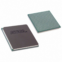
EP3SL150F780C4N Altera, EP3SL150F780C4N Datasheet - Page 273

EP3SL150F780C4N
Manufacturer Part Number
EP3SL150F780C4N
Description
IC STRATIX III FPGA 150K 780FBGA
Manufacturer
Altera
Series
Stratix® IIIr
Datasheets
1.EP3SL150F780C4N.pdf
(16 pages)
2.EP3SL150F780C4N.pdf
(332 pages)
3.EP3SL150F780C4N.pdf
(456 pages)
4.EP3SL150F780C4N.pdf
(341 pages)
Specifications of EP3SL150F780C4N
Number Of Logic Elements/cells
142500
Number Of Labs/clbs
5700
Total Ram Bits
6390
Number Of I /o
488
Voltage - Supply
0.86 V ~ 1.15 V
Mounting Type
Surface Mount
Operating Temperature
0°C ~ 85°C
Package / Case
780-FBGA
Family Name
Stratix III
Number Of Logic Blocks/elements
142500
# I/os (max)
488
Frequency (max)
450MHz
Process Technology
65nm
Operating Supply Voltage (typ)
1.1V
Logic Cells
142500
Ram Bits
6543360
Operating Supply Voltage (min)
1.05V
Operating Supply Voltage (max)
1.15V
Operating Temp Range
0C to 85C
Operating Temperature Classification
Commercial
Mounting
Surface Mount
Pin Count
780
Package Type
FC-FBGA
For Use With
544-2568 - KIT DEVELOPMENT STRATIX III
Lead Free Status / RoHS Status
Lead free / RoHS Compliant
Number Of Gates
-
Lead Free Status / Rohs Status
Compliant
Other names
544-2403
EP3SL150F780C4NES
EP3SL150F780C4NES
Available stocks
Company
Part Number
Manufacturer
Quantity
Price
Company:
Part Number:
EP3SL150F780C4N
Manufacturer:
ALTERA
Quantity:
3 000
- EP3SL150F780C4N PDF datasheet
- EP3SL150F780C4N PDF datasheet #2
- EP3SL150F780C4N PDF datasheet #3
- EP3SL150F780C4N PDF datasheet #4
- Current page: 273 of 456
- Download datasheet (7Mb)
Chapter 8: External Memory Interfaces in Stratix III Devices
Stratix III External Memory Interface Features
© March 2010 Altera Corporation
Table 8–9. DLL Reference Clock Input for EP3SL200, EP3SE260 and EP3SL340 Devices
(2)
Figure 8–12
into the DLL to a chain of up to 16 delay elements. The phase comparator compares
the signal coming out of the end of the delay chain block to the input reference clock.
The phase comparator then issues the upndn signal to the Gray-code counter. This
signal increments or decrements a 6-bit delay setting (DQS delay settings) that
increases or decreases the delay through the delay element chain to bring the input
reference clock and the signals coming out of the delay element chain in phase.
DLL0
DLL1
DLL2
DLL3
Notes to
(1) PLLs L1, L3, L4, B2, R1, R3, R4, and T2 are not available for the EP3SL200 H780 package.
(2) PLLs L1, L4, R1 and R4 are not available for the EP3SL200 F1152 package.
DLL
Table
shows a simple block diagram of the DLL. The input reference clock goes
8–9:
(Top/Bottom)
CLK12P
CLK13P
CLK14P
CLK15P
CLK12P
CLK13P
CLK14P
CLK15P
CLK4P
CLK5P
CLK6P
CLK7P
CLK4P
CLK5P
CLK6P
CLK7P
CLKIN
(Left/Right)
CLK10P
CLK11P
CLK10P
CLK11P
CLK0P
CLK1P
CLK2P
CLK3P
CLK0P
CLK1P
CLK2P
CLK3P
CLK8P
CLK9P
CLK8P
CLK9P
CLKIN
(Top/Bottom)
PLL_T1
PLL_B1
PLL_B2
PLL_T2
PLL
Stratix III Device Handbook, Volume 1
(Left/Right)
PLL_R3
PLL_R4
PLL_R1
PLL_R2
PLL_L1
PLL_L2
PLL_L3
PLL_L4
PLL
(Note
8–25
1),
Related parts for EP3SL150F780C4N
Image
Part Number
Description
Manufacturer
Datasheet
Request
R

Part Number:
Description:
CYCLONE II STARTER KIT EP2C20N
Manufacturer:
Altera
Datasheet:

Part Number:
Description:
CPLD, EP610 Family, ECMOS Process, 300 Gates, 16 Macro Cells, 16 Reg., 16 User I/Os, 5V Supply, 35 Speed Grade, 24DIP
Manufacturer:
Altera Corporation
Datasheet:

Part Number:
Description:
CPLD, EP610 Family, ECMOS Process, 300 Gates, 16 Macro Cells, 16 Reg., 16 User I/Os, 5V Supply, 15 Speed Grade, 24DIP
Manufacturer:
Altera Corporation
Datasheet:

Part Number:
Description:
Manufacturer:
Altera Corporation
Datasheet:

Part Number:
Description:
CPLD, EP610 Family, ECMOS Process, 300 Gates, 16 Macro Cells, 16 Reg., 16 User I/Os, 5V Supply, 30 Speed Grade, 24DIP
Manufacturer:
Altera Corporation
Datasheet:

Part Number:
Description:
High-performance, low-power erasable programmable logic devices with 8 macrocells, 10ns
Manufacturer:
Altera Corporation
Datasheet:

Part Number:
Description:
High-performance, low-power erasable programmable logic devices with 8 macrocells, 7ns
Manufacturer:
Altera Corporation
Datasheet:

Part Number:
Description:
Classic EPLD
Manufacturer:
Altera Corporation
Datasheet:

Part Number:
Description:
High-performance, low-power erasable programmable logic devices with 8 macrocells, 10ns
Manufacturer:
Altera Corporation
Datasheet:

Part Number:
Description:
Manufacturer:
Altera Corporation
Datasheet:

Part Number:
Description:
Manufacturer:
Altera Corporation
Datasheet:

Part Number:
Description:
Manufacturer:
Altera Corporation
Datasheet:

Part Number:
Description:
CPLD, EP610 Family, ECMOS Process, 300 Gates, 16 Macro Cells, 16 Reg., 16 User I/Os, 5V Supply, 25 Speed Grade, 24DIP
Manufacturer:
Altera Corporation
Datasheet:


