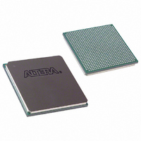
EP3SL150F780C4N Altera, EP3SL150F780C4N Datasheet - Page 448

EP3SL150F780C4N
Manufacturer Part Number
EP3SL150F780C4N
Description
IC STRATIX III FPGA 150K 780FBGA
Manufacturer
Altera
Series
Stratix® IIIr
Datasheets
1.EP3SL150F780C4N.pdf
(16 pages)
2.EP3SL150F780C4N.pdf
(332 pages)
3.EP3SL150F780C4N.pdf
(456 pages)
4.EP3SL150F780C4N.pdf
(341 pages)
Specifications of EP3SL150F780C4N
Number Of Logic Elements/cells
142500
Number Of Labs/clbs
5700
Total Ram Bits
6390
Number Of I /o
488
Voltage - Supply
0.86 V ~ 1.15 V
Mounting Type
Surface Mount
Operating Temperature
0°C ~ 85°C
Package / Case
780-FBGA
Family Name
Stratix III
Number Of Logic Blocks/elements
142500
# I/os (max)
488
Frequency (max)
450MHz
Process Technology
65nm
Operating Supply Voltage (typ)
1.1V
Logic Cells
142500
Ram Bits
6543360
Operating Supply Voltage (min)
1.05V
Operating Supply Voltage (max)
1.15V
Operating Temp Range
0C to 85C
Operating Temperature Classification
Commercial
Mounting
Surface Mount
Pin Count
780
Package Type
FC-FBGA
For Use With
544-2568 - KIT DEVELOPMENT STRATIX III
Lead Free Status / RoHS Status
Lead free / RoHS Compliant
Number Of Gates
-
Lead Free Status / Rohs Status
Compliant
Other names
544-2403
EP3SL150F780C4NES
EP3SL150F780C4NES
Available stocks
Company
Part Number
Manufacturer
Quantity
Price
Company:
Part Number:
EP3SL150F780C4N
Manufacturer:
ALTERA
Quantity:
3 000
- EP3SL150F780C4N PDF datasheet
- EP3SL150F780C4N PDF datasheet #2
- EP3SL150F780C4N PDF datasheet #3
- EP3SL150F780C4N PDF datasheet #4
- Current page: 448 of 456
- Download datasheet (7Mb)
16–4
Table 16–2. Stratix III Power Supply Requirements
Stratix III Device Handbook, Volume 1
VCCL
VCC
VCCD_PLL
VCCA_PLL
VCCPT
VCCPGM
VCCPD
VCCIO
VCC_CLKIN
VCCBAT
VREF
GND
Notes to
(1) You can minimize the number of external power sources by driving the left column and supplies with the same voltage regulator. Note that
(2) V
(3) This scheme is for VCCIO = 2.5 V.
(4) There is one VREF pin per I/O bank. Use an external power supply or a resistor divider network to supply this voltage.
Power Supply
separate power planes, decoupling capacitors, and ferrite beads are required for VCCA_PLL and VCCPT when implementing this scheme.
standards, V
CC PD
Pin
Table
can be either 2.5 V, 3.0 V, or 3.3 V. For a 3.3-V standard, V
f
f
16–2:
CC PD
= 2.5 V.
Board Connection
VCCA_PLL
Recommended
VCCPD
VCCD_PLL
VREF
VCCIO
For possible values of each power supply, refer to the
of Stratix III Devices
For detailed guidelines about how to connect and isolate VCCL and VCC power supply
pins, refer to the
VCCPGM
VCCBAT
VCCL
VCC
GND
(4)
(2)
(3)
(1)
Selectable core voltage power supply
I/O registers power supply
PLL digital power supply
PLL analog power supply
Power supply for programmable power technology
Configuration pins power supply
I/O pre-driver power supply
I/O power supply
Differential clock input pins power supply (top and bottom I/O banks only)
Battery back-up power supply for design security volatile key register
Power supply for voltage-referenced I/O standards
Ground
Stratix III Device Family Pin Connections
chapter in volume 2 of the Stratix III Device Handbook.
Chapter 16: Programmable Power and Temperature-Sensing Diodes in Stratix III Devices
CC PD
= 3.3 V. For a 3.0-V I/O standard, V
Description
Stratix III External Power Supply Requirements
DC and Switching Characteristics
Guidelines.
C CP D
© February 2009 Altera Corporation
= 3.0 V. For 2.5 V and below I/O
Related parts for EP3SL150F780C4N
Image
Part Number
Description
Manufacturer
Datasheet
Request
R

Part Number:
Description:
CYCLONE II STARTER KIT EP2C20N
Manufacturer:
Altera
Datasheet:

Part Number:
Description:
CPLD, EP610 Family, ECMOS Process, 300 Gates, 16 Macro Cells, 16 Reg., 16 User I/Os, 5V Supply, 35 Speed Grade, 24DIP
Manufacturer:
Altera Corporation
Datasheet:

Part Number:
Description:
CPLD, EP610 Family, ECMOS Process, 300 Gates, 16 Macro Cells, 16 Reg., 16 User I/Os, 5V Supply, 15 Speed Grade, 24DIP
Manufacturer:
Altera Corporation
Datasheet:

Part Number:
Description:
Manufacturer:
Altera Corporation
Datasheet:

Part Number:
Description:
CPLD, EP610 Family, ECMOS Process, 300 Gates, 16 Macro Cells, 16 Reg., 16 User I/Os, 5V Supply, 30 Speed Grade, 24DIP
Manufacturer:
Altera Corporation
Datasheet:

Part Number:
Description:
High-performance, low-power erasable programmable logic devices with 8 macrocells, 10ns
Manufacturer:
Altera Corporation
Datasheet:

Part Number:
Description:
High-performance, low-power erasable programmable logic devices with 8 macrocells, 7ns
Manufacturer:
Altera Corporation
Datasheet:

Part Number:
Description:
Classic EPLD
Manufacturer:
Altera Corporation
Datasheet:

Part Number:
Description:
High-performance, low-power erasable programmable logic devices with 8 macrocells, 10ns
Manufacturer:
Altera Corporation
Datasheet:

Part Number:
Description:
Manufacturer:
Altera Corporation
Datasheet:

Part Number:
Description:
Manufacturer:
Altera Corporation
Datasheet:

Part Number:
Description:
Manufacturer:
Altera Corporation
Datasheet:

Part Number:
Description:
CPLD, EP610 Family, ECMOS Process, 300 Gates, 16 Macro Cells, 16 Reg., 16 User I/Os, 5V Supply, 25 Speed Grade, 24DIP
Manufacturer:
Altera Corporation
Datasheet:


