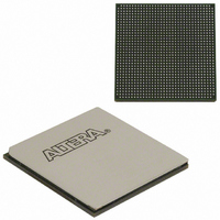
EP3SL150F1152C3N Altera, EP3SL150F1152C3N Datasheet - Page 11

EP3SL150F1152C3N
Manufacturer Part Number
EP3SL150F1152C3N
Description
IC STRATX III FPGA 150K 1152FBGA
Manufacturer
Altera
Series
Stratix® IIIr
Datasheets
1.EP3SL150F780C4N.pdf
(16 pages)
2.EP3SL150F780C4N.pdf
(332 pages)
3.EP3SL150F780C4N.pdf
(456 pages)
Specifications of EP3SL150F1152C3N
Number Of Logic Elements/cells
142500
Number Of Labs/clbs
5700
Total Ram Bits
6390
Number Of I /o
744
Voltage - Supply
0.86 V ~ 1.15 V
Mounting Type
Surface Mount
Operating Temperature
0°C ~ 85°C
Package / Case
1152-FBGA
For Use With
544-2568 - KIT DEVELOPMENT STRATIX III
Lead Free Status / RoHS Status
Lead free / RoHS Compliant
Number Of Gates
-
Other names
544-2408
EP3SL150F1152C3NES
EP3SL150F1152C3NES
Available stocks
Company
Part Number
Manufacturer
Quantity
Price
Company:
Part Number:
EP3SL150F1152C3N
Manufacturer:
ALTERA
Quantity:
490
- Current page: 11 of 332
- Download datasheet (4Mb)
Chapter 1: Stratix III Device Datasheet: DC and Switching Characteristics
Electrical Characteristics
Table 1–15. Single-Ended SSTL and HSTL I/O Standards Signal Specifications
Table 1–16. Differential SSTL I/O Standard Specifications
Table 1–17. Differential HSTL I/O Standards Specifications
Table 1–18. Differential I/O Standard Specifications (Part 1 of 2)
© July 2010 Altera Corporation
HSTL-12
CLASS II
Note to
(1) Use the current strength settings that are equal or larger than the I
SSTL-2
CLASS I, II
SSTL-18
CLASS I, II
SSTL-15
CLASS I, II
HSTL-18
CLASS I, II
HSTL-15
CLASS I, II
HSTL-12
CLASS I, II
2.5 V LVDS
(Row I/O)
Standard
Standard
I/O Standard
Standard
I/O
I/O
OCT or lower current strengths may provide better signal integrity and lower power.
I/O
Table
1–15:
2.375
1.425
-0.15
1.71
Min
Min
2.375
2.375
Min
1.425
1.71
1.14
Min
V
IL(DC)
V
V
CCIO
Typ
2.5
1.8
1.5
CCIO
Typ
V
2.5
2.5
Refer to the figures for “Differential I/O Standards” in
the receiver input and transmitter output waveforms, and for all the differential I/O
standards (LVDS, mini-LVDS, RSDS). V
column clock input pins. V
column I/Os.
V
(V)
REF
(V)
CCIO
Max
Typ
1.8
1.5
1.2
(V)
-0.08
(V)
2.625
1.575
Max
1.89
2.625
2.625
Max
1.575
1.89
1.26
Max
V
REF
0.25
Min
Min
0.1
0.1
0.3
0.2
Min
V
+0.08
0.16
SWING (DC)
Min
0.2
0.2
V
DIF(DC)
V
Condition
IH(DC)
+ 0.6
+ 0.6
V
V
Max
V
V
V
(V)
—
CM
CM
+ 0.3
CCIO
CCIO
ID
Max
(V)
V
—
—
= 1.25
= 1.25
(V)
(V)
CCIO
V
CCIO
Max
(1)
+ 0.15
-0.175
V
V
- 0.2
Min
0.78
0.68
CCIO
CCIO
Min
—
—
CCPD
/2
/2
Max
—
—
is the power supply for the row I/Os and all other
OL
0.5* V
V
V
V
V
V
and I
Typ
X(AC)
REF
X (AC)
CCIO
—
—
Typ
IL(AC)
—
—
Max
0.05
1.05
Min
/2
-0.15
(6)
(6)
(V)
(V)
OH
CCIO
(V)
values listed to meet the V
CC_CLKIN
+ 0.175
V
V
+ 0.2
Max
1.12
Condition
Max
D
0.9
D
—
CCIO
CCIO
V
—
V
max
max
V
ICM(DC)
Mbps
Mbps
REF
/2
/2
700
IH(AC)
> 700
Min
+ 0.15
is the power supply for the differential
(V)
(Note 1)
0.4* V
(V)
0.78
0.68
Min
0.62
0.35
Min
0.5
V
CCIO
SWING(AC)
Max
1.55
1.8
(6)
(6)
0.25* V
“Glossary” on page 1–326
V
(Part 2 of 2)
Max
OL
V
0.5* V
OL
CM(DC)
(V)
(V)
+ 0.6
+ 0.6
Max
Stratix III Device Handbook, Volume 2
V
V
Typ
—
and V
—
—
0.247
0.247
CCIO
CCIO
CCIO
Min
(V)
CCIO
OH
V
0.75 * V
-0.125
- 0.15
specifications for each line.
OD
V
V
Min
0.6* V
V
Typ
CCIO
CCIO
—
—
—
(V)
Min
OH
1.12
Max
0.9
/2
/2
(V)
(2)
CCIO
CCIO
V
Max
OX (AC)
0.6
0.6
V
Typ
—
—
CCIO
Min
(mA)
0.4
0.4
0.3
IOL
/2
16
(V)
V
DIF(AC)
1.125 1.25 1.375
1.125 1.25 1.375
V
+0.125
Min
+ 0.48
V
for
Max
CCIO
0.15
Max
1–11
(mA)
(V)
CCIO
V
—
-16
—
—
I
/2 +
CCIO
OH
V
/2
OCM
Typ
(V)
(2)
Max
Related parts for EP3SL150F1152C3N
Image
Part Number
Description
Manufacturer
Datasheet
Request
R

Part Number:
Description:
CYCLONE II STARTER KIT EP2C20N
Manufacturer:
Altera
Datasheet:

Part Number:
Description:
CPLD, EP610 Family, ECMOS Process, 300 Gates, 16 Macro Cells, 16 Reg., 16 User I/Os, 5V Supply, 35 Speed Grade, 24DIP
Manufacturer:
Altera Corporation
Datasheet:

Part Number:
Description:
CPLD, EP610 Family, ECMOS Process, 300 Gates, 16 Macro Cells, 16 Reg., 16 User I/Os, 5V Supply, 15 Speed Grade, 24DIP
Manufacturer:
Altera Corporation
Datasheet:

Part Number:
Description:
Manufacturer:
Altera Corporation
Datasheet:

Part Number:
Description:
CPLD, EP610 Family, ECMOS Process, 300 Gates, 16 Macro Cells, 16 Reg., 16 User I/Os, 5V Supply, 30 Speed Grade, 24DIP
Manufacturer:
Altera Corporation
Datasheet:

Part Number:
Description:
High-performance, low-power erasable programmable logic devices with 8 macrocells, 10ns
Manufacturer:
Altera Corporation
Datasheet:

Part Number:
Description:
High-performance, low-power erasable programmable logic devices with 8 macrocells, 7ns
Manufacturer:
Altera Corporation
Datasheet:

Part Number:
Description:
Classic EPLD
Manufacturer:
Altera Corporation
Datasheet:

Part Number:
Description:
High-performance, low-power erasable programmable logic devices with 8 macrocells, 10ns
Manufacturer:
Altera Corporation
Datasheet:

Part Number:
Description:
Manufacturer:
Altera Corporation
Datasheet:

Part Number:
Description:
Manufacturer:
Altera Corporation
Datasheet:

Part Number:
Description:
Manufacturer:
Altera Corporation
Datasheet:

Part Number:
Description:
CPLD, EP610 Family, ECMOS Process, 300 Gates, 16 Macro Cells, 16 Reg., 16 User I/Os, 5V Supply, 25 Speed Grade, 24DIP
Manufacturer:
Altera Corporation
Datasheet:


