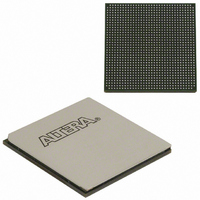
EP3SL150F1152C3N Altera, EP3SL150F1152C3N Datasheet - Page 155

EP3SL150F1152C3N
Manufacturer Part Number
EP3SL150F1152C3N
Description
IC STRATX III FPGA 150K 1152FBGA
Manufacturer
Altera
Series
Stratix® IIIr
Datasheets
1.EP3SL150F780C4N.pdf
(16 pages)
2.EP3SL150F780C4N.pdf
(332 pages)
3.EP3SL150F780C4N.pdf
(456 pages)
Specifications of EP3SL150F1152C3N
Number Of Logic Elements/cells
142500
Number Of Labs/clbs
5700
Total Ram Bits
6390
Number Of I /o
744
Voltage - Supply
0.86 V ~ 1.15 V
Mounting Type
Surface Mount
Operating Temperature
0°C ~ 85°C
Package / Case
1152-FBGA
For Use With
544-2568 - KIT DEVELOPMENT STRATIX III
Lead Free Status / RoHS Status
Lead free / RoHS Compliant
Number Of Gates
-
Other names
544-2408
EP3SL150F1152C3NES
EP3SL150F1152C3NES
Available stocks
Company
Part Number
Manufacturer
Quantity
Price
Company:
Part Number:
EP3SL150F1152C3N
Manufacturer:
ALTERA
Quantity:
490
- Current page: 155 of 456
- Download datasheet (7Mb)
Chapter 6: Clock Networks and PLLs in Stratix III Devices
Clock Networks in Stratix III Devices
Figure 6–10. Stratix III Dual-Regional Clock Region
© July 2010
Altera Corporation
In order to form the entire device clock region, a source (not necessarily a clock signal)
drives a global clock network that can be routed through the entire device. This clock
region has the maximum delay compared to other clock regions but allows the signal
to reach every destination within the device. This is a good option for routing global
reset/clear signals or routing clocks throughout the device.
In order to form a regional clock region, a source drives a single-quadrant of the
device. This clock region provides the lowest skew within a quadrant and is a good
option if all destinations are within a single device quadrant.
To form a dual-regional clock region, a single source (a clock pin or PLL output)
generates a dual-regional clock by driving two regional clock networks (one from
each quadrant). This technique allows destinations across two device quadrants to
use the same low-skew clock. The routing of this signal on an entire side has
approximately the same delay as in a regional clock region. Internal logic can also
drive a dual-regional clock network. Corner PLL outputs only span one quadrant and
hence cannot generate a dual-regional clock network.
dual-regional clock region.
Clock Network Sources
In Stratix III devices, clock input pins, PLL outputs, and internal logic can drive the
global and regional clock networks. Refer to
between dedicated CLK[0..15] pins and the global and regional clock networks.
Dedicated Clock Inputs Pins
The CLK pins can either be differential clocks or single-ended clocks. Stratix III devices
support 16 differential clock inputs or 32 single-ended clock inputs. You can also use
the dedicated clock input pins CLK[15..0] for high fan-out control signals such as
asynchronous clears, presets, and clock enables for protocol signals such as TRDY and
IRDY for PCI through global or regional clock networks.
Table 6–2
Clock pins or PLL outputs
can drive half of the device to
create side-wide clocking
regions for improved
interface timing.
to
Figure 6–10
Table 6–6
Stratix III Device Handbook, Volume 1
for the connectivity
shows the
6–7
Related parts for EP3SL150F1152C3N
Image
Part Number
Description
Manufacturer
Datasheet
Request
R

Part Number:
Description:
CYCLONE II STARTER KIT EP2C20N
Manufacturer:
Altera
Datasheet:

Part Number:
Description:
CPLD, EP610 Family, ECMOS Process, 300 Gates, 16 Macro Cells, 16 Reg., 16 User I/Os, 5V Supply, 35 Speed Grade, 24DIP
Manufacturer:
Altera Corporation
Datasheet:

Part Number:
Description:
CPLD, EP610 Family, ECMOS Process, 300 Gates, 16 Macro Cells, 16 Reg., 16 User I/Os, 5V Supply, 15 Speed Grade, 24DIP
Manufacturer:
Altera Corporation
Datasheet:

Part Number:
Description:
Manufacturer:
Altera Corporation
Datasheet:

Part Number:
Description:
CPLD, EP610 Family, ECMOS Process, 300 Gates, 16 Macro Cells, 16 Reg., 16 User I/Os, 5V Supply, 30 Speed Grade, 24DIP
Manufacturer:
Altera Corporation
Datasheet:

Part Number:
Description:
High-performance, low-power erasable programmable logic devices with 8 macrocells, 10ns
Manufacturer:
Altera Corporation
Datasheet:

Part Number:
Description:
High-performance, low-power erasable programmable logic devices with 8 macrocells, 7ns
Manufacturer:
Altera Corporation
Datasheet:

Part Number:
Description:
Classic EPLD
Manufacturer:
Altera Corporation
Datasheet:

Part Number:
Description:
High-performance, low-power erasable programmable logic devices with 8 macrocells, 10ns
Manufacturer:
Altera Corporation
Datasheet:

Part Number:
Description:
Manufacturer:
Altera Corporation
Datasheet:

Part Number:
Description:
Manufacturer:
Altera Corporation
Datasheet:

Part Number:
Description:
Manufacturer:
Altera Corporation
Datasheet:

Part Number:
Description:
CPLD, EP610 Family, ECMOS Process, 300 Gates, 16 Macro Cells, 16 Reg., 16 User I/Os, 5V Supply, 25 Speed Grade, 24DIP
Manufacturer:
Altera Corporation
Datasheet:


