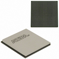
EP3SL150F1152C3N Altera, EP3SL150F1152C3N Datasheet - Page 156

EP3SL150F1152C3N
Manufacturer Part Number
EP3SL150F1152C3N
Description
IC STRATX III FPGA 150K 1152FBGA
Manufacturer
Altera
Series
Stratix® IIIr
Datasheets
1.EP3SL150F780C4N.pdf
(16 pages)
2.EP3SL150F780C4N.pdf
(332 pages)
3.EP3SL150F780C4N.pdf
(456 pages)
Specifications of EP3SL150F1152C3N
Number Of Logic Elements/cells
142500
Number Of Labs/clbs
5700
Total Ram Bits
6390
Number Of I /o
744
Voltage - Supply
0.86 V ~ 1.15 V
Mounting Type
Surface Mount
Operating Temperature
0°C ~ 85°C
Package / Case
1152-FBGA
For Use With
544-2568 - KIT DEVELOPMENT STRATIX III
Lead Free Status / RoHS Status
Lead free / RoHS Compliant
Number Of Gates
-
Other names
544-2408
EP3SL150F1152C3NES
EP3SL150F1152C3NES
Available stocks
Company
Part Number
Manufacturer
Quantity
Price
Company:
Part Number:
EP3SL150F1152C3N
Manufacturer:
ALTERA
Quantity:
490
- Current page: 156 of 456
- Download datasheet (7Mb)
6–8
Table 6–2. Clock Input Pin Connectivity to Global Clock Networks
Stratix III Device Handbook, Volume 1
GCLK0
GCLK1
GCLK2
GCLK3
GCLK4
GCLK5
GCLK6
GCLK7
GCLK8
GCLK9
GCLK10
GCLK11
GCLK12
GCLK13
GCLK14
GCLK15
Clock Resources
1
1
Logic Array Blocks (LABs)
You can also drive each global and regional clock network via LAB-routing to enable
internal logic to drive a high fan-out, low-skew signal.
Stratix III device PLLs cannot be driven by internally generated GCLKs or RCLKs.
The input clock to the PLL must come from dedicated clock input pins/PLL-fed
GCLKs or RCLKs only.
A spine clock is essentially another layer of routing below global/regional and
periphery clocks before each clock is connected to the clock routing for each LAB row.
The settings for a spine clock are transparent to all users. The Quartus II software
takes care of the spine clock routing based on the global/regional and periphery
clocks.
PLL Clock Outputs
Stratix III PLLs can drive both GCLK and RCLK networks, as detailed in
page 6–12
Table 6–2
v
v
v
v
—
—
—
—
—
—
—
—
—
—
—
—
0
v
v
v
v
—
—
—
—
—
—
—
—
—
—
—
—
1
lists the connection between the dedicated clock input pins and GCLKs.
and
v
v
v
v
—
—
—
—
—
—
—
—
—
—
—
—
2
Table 6–9 on page
v
v
v
v
—
—
—
—
—
—
—
—
—
—
—
—
3
v
v
v
v
—
—
—
—
—
—
—
—
—
—
—
—
4
—
—
—
v
v
v
v
—
—
—
—
—
—
—
—
—
5
v
v
v
v
—
—
—
—
—
—
—
—
—
—
—
—
6–13.
6
CLK (p/n Pins)
—
—
—
—
v
v
v
v
—
—
—
—
—
—
—
—
7
Chapter 6: Clock Networks and PLLs in Stratix III Devices
v
v
v
v
—
—
—
—
—
—
—
—
—
—
—
—
8
—
—
—
—
—
—
—
—
v
v
v
v
—
—
—
—
9
v
v
v
v
10
—
—
—
—
—
—
—
—
—
—
—
—
Clock Networks in Stratix III Devices
v
v
v
v
11
—
—
—
—
—
—
—
—
—
—
—
—
© July 2010 Altera Corporation
12
—
—
—
—
—
—
—
—
—
—
—
—
v
v
v
v
v
v
v
v
13
—
—
—
—
—
—
—
—
—
—
—
—
Table 6–8 on
v
v
v
v
14
—
—
—
—
—
—
—
—
—
—
—
—
v
v
v
v
15
—
—
—
—
—
—
—
—
—
—
—
—
Related parts for EP3SL150F1152C3N
Image
Part Number
Description
Manufacturer
Datasheet
Request
R

Part Number:
Description:
CYCLONE II STARTER KIT EP2C20N
Manufacturer:
Altera
Datasheet:

Part Number:
Description:
CPLD, EP610 Family, ECMOS Process, 300 Gates, 16 Macro Cells, 16 Reg., 16 User I/Os, 5V Supply, 35 Speed Grade, 24DIP
Manufacturer:
Altera Corporation
Datasheet:

Part Number:
Description:
CPLD, EP610 Family, ECMOS Process, 300 Gates, 16 Macro Cells, 16 Reg., 16 User I/Os, 5V Supply, 15 Speed Grade, 24DIP
Manufacturer:
Altera Corporation
Datasheet:

Part Number:
Description:
Manufacturer:
Altera Corporation
Datasheet:

Part Number:
Description:
CPLD, EP610 Family, ECMOS Process, 300 Gates, 16 Macro Cells, 16 Reg., 16 User I/Os, 5V Supply, 30 Speed Grade, 24DIP
Manufacturer:
Altera Corporation
Datasheet:

Part Number:
Description:
High-performance, low-power erasable programmable logic devices with 8 macrocells, 10ns
Manufacturer:
Altera Corporation
Datasheet:

Part Number:
Description:
High-performance, low-power erasable programmable logic devices with 8 macrocells, 7ns
Manufacturer:
Altera Corporation
Datasheet:

Part Number:
Description:
Classic EPLD
Manufacturer:
Altera Corporation
Datasheet:

Part Number:
Description:
High-performance, low-power erasable programmable logic devices with 8 macrocells, 10ns
Manufacturer:
Altera Corporation
Datasheet:

Part Number:
Description:
Manufacturer:
Altera Corporation
Datasheet:

Part Number:
Description:
Manufacturer:
Altera Corporation
Datasheet:

Part Number:
Description:
Manufacturer:
Altera Corporation
Datasheet:

Part Number:
Description:
CPLD, EP610 Family, ECMOS Process, 300 Gates, 16 Macro Cells, 16 Reg., 16 User I/Os, 5V Supply, 25 Speed Grade, 24DIP
Manufacturer:
Altera Corporation
Datasheet:


