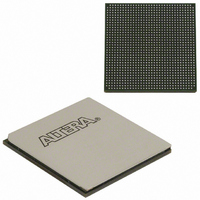
EP3SL150F1152C3N Altera, EP3SL150F1152C3N Datasheet - Page 182

EP3SL150F1152C3N
Manufacturer Part Number
EP3SL150F1152C3N
Description
IC STRATX III FPGA 150K 1152FBGA
Manufacturer
Altera
Series
Stratix® IIIr
Datasheets
1.EP3SL150F780C4N.pdf
(16 pages)
2.EP3SL150F780C4N.pdf
(332 pages)
3.EP3SL150F780C4N.pdf
(456 pages)
Specifications of EP3SL150F1152C3N
Number Of Logic Elements/cells
142500
Number Of Labs/clbs
5700
Total Ram Bits
6390
Number Of I /o
744
Voltage - Supply
0.86 V ~ 1.15 V
Mounting Type
Surface Mount
Operating Temperature
0°C ~ 85°C
Package / Case
1152-FBGA
For Use With
544-2568 - KIT DEVELOPMENT STRATIX III
Lead Free Status / RoHS Status
Lead free / RoHS Compliant
Number Of Gates
-
Other names
544-2408
EP3SL150F1152C3NES
EP3SL150F1152C3NES
Available stocks
Company
Part Number
Manufacturer
Quantity
Price
Company:
Part Number:
EP3SL150F1152C3N
Manufacturer:
ALTERA
Quantity:
490
- Current page: 182 of 456
- Download datasheet (7Mb)
6–34
Figure 6–32. Automatic Clock Switchover Circuit Block Diagram
Stratix III Device Handbook, Volume 1
inclk0
inclk1
The following clock switchover modes are supported in Stratix III PLLs:
■
■
■
Stratix III device PLLs support a fully configurable clock switchover capability.
Figure 6–32
When the current reference clock is not present, the clock sense block automatically
switches to the backup clock for PLL reference. The clock switchover circuit also sends
out three status signals—clkbad[0], clkbad[1], and activeclock—from the
PLL to implement a custom switchover circuit in the logic array. You can select a clock
source as the backup clock by connecting it to the inclk1 port of the PLL in your
design.
Automatic Clock Switchover
Use the switchover circuitry to automatically switch between inclk0 and inclk1
when the current reference clock to the PLL stops toggling. For example, in
applications that require a redundant clock with the same frequency as the reference
clock, the switchover state machine generates a signal (clksw) that controls the
multiplexer select input as shown in
reference clock for the PLL. When using the automatic switchover mode, you can
switch back and forth between inclk0 and inclk1 clocks any number of times,
when one of the two clocks fails and the other clock is available.
Automatic switchover—The clock sense circuit monitors the current reference
clock and if it stops toggling, automatically switches to the other clock inclk0 or
inclk1.
Manual clock switchover—Clock switchover is controlled via the clkswitch
signal in this mode. When the clkswitch signal goes from logic low to logic
high, and stays high for at least three clock cycles, the reference clock to the PLL is
switched from inclk0 to inclk1, or vice-versa.
Automatic switchover with manual override—This mode combines Modes 1 and
2. When the clkswitch signal goes high, it overrides automatic clock switchover
mode.
muxout
shows the block diagram of the switchover circuit built into the PLL.
clksw
n Counter
Sense
Clock
refclk
Figure
Switchover
Machine
State
Chapter 6: Clock Networks and PLLs in Stratix III Devices
6–32. In this case, inclk1 becomes the
Clock Switch
Control Logic
PFD
fbclk
clkbad0
clkbad1
activeclock
clkswitch
© July 2010 Altera Corporation
PLLs in Stratix III Devices
Related parts for EP3SL150F1152C3N
Image
Part Number
Description
Manufacturer
Datasheet
Request
R

Part Number:
Description:
CYCLONE II STARTER KIT EP2C20N
Manufacturer:
Altera
Datasheet:

Part Number:
Description:
CPLD, EP610 Family, ECMOS Process, 300 Gates, 16 Macro Cells, 16 Reg., 16 User I/Os, 5V Supply, 35 Speed Grade, 24DIP
Manufacturer:
Altera Corporation
Datasheet:

Part Number:
Description:
CPLD, EP610 Family, ECMOS Process, 300 Gates, 16 Macro Cells, 16 Reg., 16 User I/Os, 5V Supply, 15 Speed Grade, 24DIP
Manufacturer:
Altera Corporation
Datasheet:

Part Number:
Description:
Manufacturer:
Altera Corporation
Datasheet:

Part Number:
Description:
CPLD, EP610 Family, ECMOS Process, 300 Gates, 16 Macro Cells, 16 Reg., 16 User I/Os, 5V Supply, 30 Speed Grade, 24DIP
Manufacturer:
Altera Corporation
Datasheet:

Part Number:
Description:
High-performance, low-power erasable programmable logic devices with 8 macrocells, 10ns
Manufacturer:
Altera Corporation
Datasheet:

Part Number:
Description:
High-performance, low-power erasable programmable logic devices with 8 macrocells, 7ns
Manufacturer:
Altera Corporation
Datasheet:

Part Number:
Description:
Classic EPLD
Manufacturer:
Altera Corporation
Datasheet:

Part Number:
Description:
High-performance, low-power erasable programmable logic devices with 8 macrocells, 10ns
Manufacturer:
Altera Corporation
Datasheet:

Part Number:
Description:
Manufacturer:
Altera Corporation
Datasheet:

Part Number:
Description:
Manufacturer:
Altera Corporation
Datasheet:

Part Number:
Description:
Manufacturer:
Altera Corporation
Datasheet:

Part Number:
Description:
CPLD, EP610 Family, ECMOS Process, 300 Gates, 16 Macro Cells, 16 Reg., 16 User I/Os, 5V Supply, 25 Speed Grade, 24DIP
Manufacturer:
Altera Corporation
Datasheet:


