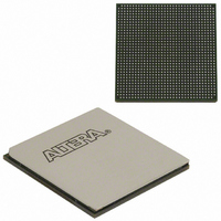
EP3SL150F1152C3N Altera, EP3SL150F1152C3N Datasheet - Page 193

EP3SL150F1152C3N
Manufacturer Part Number
EP3SL150F1152C3N
Description
IC STRATX III FPGA 150K 1152FBGA
Manufacturer
Altera
Series
Stratix® IIIr
Datasheets
1.EP3SL150F780C4N.pdf
(16 pages)
2.EP3SL150F780C4N.pdf
(332 pages)
3.EP3SL150F780C4N.pdf
(456 pages)
Specifications of EP3SL150F1152C3N
Number Of Logic Elements/cells
142500
Number Of Labs/clbs
5700
Total Ram Bits
6390
Number Of I /o
744
Voltage - Supply
0.86 V ~ 1.15 V
Mounting Type
Surface Mount
Operating Temperature
0°C ~ 85°C
Package / Case
1152-FBGA
For Use With
544-2568 - KIT DEVELOPMENT STRATIX III
Lead Free Status / RoHS Status
Lead free / RoHS Compliant
Number Of Gates
-
Other names
544-2408
EP3SL150F1152C3NES
EP3SL150F1152C3NES
Available stocks
Company
Part Number
Manufacturer
Quantity
Price
Company:
Part Number:
EP3SL150F1152C3N
Manufacturer:
ALTERA
Quantity:
490
- Current page: 193 of 456
- Download datasheet (7Mb)
Chapter 6: Clock Networks and PLLs in Stratix III Devices
PLLs in Stratix III Devices
Figure 6–41. PLL Reconfiguration Waveform
© July 2010
CONFIGUPDATE
SCANDATAOUT
SCANCLKENA
SCANDONE
SCANDATA
SCANCLK
ARESET
Altera Corporation
1
Figure 6–41
When you reconfigure the counter clock frequency, you cannot reconfigure the
corresponding counter phase shift settings using the same interface. Instead,
reconfigure the phase shifts in real time using the dynamic phase shift reconfiguration
interface. If you reconfigure the counter frequency, but wish to keep the same
non-zero phase shift setting (for example, 90 degrees) on the clock output, you must
reconfigure the phase shift immediately after reconfiguring the counter clock
frequency.
Post-Scale Counters (C0 to C9)
The multiply or divide values and duty cycle of post-scale counters can be
reconfigured in real time. Each counter has an 8-bit high-time setting and an 8-bit
low-time setting. The duty cycle is the ratio of output
high- or low-time to the total cycle time, which is the sum of the two. Additionally,
these counters have two control bits, rbypass, for bypassing the counter, and
rselodd, to select the output clock duty cycle.
When the rbypass bit is set to 1, it bypasses the counter, resulting in a divide by 1.
When this bit is set to 0, the high- and low-time counters are added to compute the
effective division of the VCO output frequency. For example, if the post-scale divide
factor is 10, the high- and low-count values could be set to 5 and 5, respectively, to
achieve a 50-50% duty cycle. The PLL implements this duty cycle by transitioning the
output clock from high to low on the rising edge of the VCO output clock. However, a
4 and 6 setting for the high- and low-count values, respectively, would produce an
output clock with 40-60% duty cycle.
Dn_old
Dn
shows a functional simulation of the PLL reconfiguration feature.
D0_old
D0
Stratix III Device Handbook, Volume 1
Dn
6–45
Related parts for EP3SL150F1152C3N
Image
Part Number
Description
Manufacturer
Datasheet
Request
R

Part Number:
Description:
CYCLONE II STARTER KIT EP2C20N
Manufacturer:
Altera
Datasheet:

Part Number:
Description:
CPLD, EP610 Family, ECMOS Process, 300 Gates, 16 Macro Cells, 16 Reg., 16 User I/Os, 5V Supply, 35 Speed Grade, 24DIP
Manufacturer:
Altera Corporation
Datasheet:

Part Number:
Description:
CPLD, EP610 Family, ECMOS Process, 300 Gates, 16 Macro Cells, 16 Reg., 16 User I/Os, 5V Supply, 15 Speed Grade, 24DIP
Manufacturer:
Altera Corporation
Datasheet:

Part Number:
Description:
Manufacturer:
Altera Corporation
Datasheet:

Part Number:
Description:
CPLD, EP610 Family, ECMOS Process, 300 Gates, 16 Macro Cells, 16 Reg., 16 User I/Os, 5V Supply, 30 Speed Grade, 24DIP
Manufacturer:
Altera Corporation
Datasheet:

Part Number:
Description:
High-performance, low-power erasable programmable logic devices with 8 macrocells, 10ns
Manufacturer:
Altera Corporation
Datasheet:

Part Number:
Description:
High-performance, low-power erasable programmable logic devices with 8 macrocells, 7ns
Manufacturer:
Altera Corporation
Datasheet:

Part Number:
Description:
Classic EPLD
Manufacturer:
Altera Corporation
Datasheet:

Part Number:
Description:
High-performance, low-power erasable programmable logic devices with 8 macrocells, 10ns
Manufacturer:
Altera Corporation
Datasheet:

Part Number:
Description:
Manufacturer:
Altera Corporation
Datasheet:

Part Number:
Description:
Manufacturer:
Altera Corporation
Datasheet:

Part Number:
Description:
Manufacturer:
Altera Corporation
Datasheet:

Part Number:
Description:
CPLD, EP610 Family, ECMOS Process, 300 Gates, 16 Macro Cells, 16 Reg., 16 User I/Os, 5V Supply, 25 Speed Grade, 24DIP
Manufacturer:
Altera Corporation
Datasheet:


