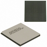
EP3SL150F1152C3N Altera, EP3SL150F1152C3N Datasheet - Page 244

EP3SL150F1152C3N
Manufacturer Part Number
EP3SL150F1152C3N
Description
IC STRATX III FPGA 150K 1152FBGA
Manufacturer
Altera
Series
Stratix® IIIr
Datasheets
1.EP3SL150F780C4N.pdf
(16 pages)
2.EP3SL150F780C4N.pdf
(332 pages)
3.EP3SL150F780C4N.pdf
(456 pages)
Specifications of EP3SL150F1152C3N
Number Of Logic Elements/cells
142500
Number Of Labs/clbs
5700
Total Ram Bits
6390
Number Of I /o
744
Voltage - Supply
0.86 V ~ 1.15 V
Mounting Type
Surface Mount
Operating Temperature
0°C ~ 85°C
Package / Case
1152-FBGA
For Use With
544-2568 - KIT DEVELOPMENT STRATIX III
Lead Free Status / RoHS Status
Lead free / RoHS Compliant
Number Of Gates
-
Other names
544-2408
EP3SL150F1152C3NES
EP3SL150F1152C3NES
Available stocks
Company
Part Number
Manufacturer
Quantity
Price
Company:
Part Number:
EP3SL150F1152C3N
Manufacturer:
ALTERA
Quantity:
490
- Current page: 244 of 456
- Download datasheet (7Mb)
7–40
I/O Termination
I/O Banks Restrictions
Stratix III Device Handbook, Volume 1
f
I/O termination requirements for single-ended and differential I/O standards are
discussed in this section.
Single-Ended I/O Standards
Although single-ended, non-voltage-referenced I/O standards do not require
termination, impedance matching may be necessary to reduce reflections and
improve signal integrity.
Voltage-referenced I/O standards require both an input reference voltage, V
termination voltage, V
termination voltage of the transmitting device. Each voltage-referenced I/O standard
requires a unique termination setup. For example, a proper resistive signal
termination scheme is critical in SSTL2 standards to produce a reliable DDR memory
system with superior noise margin.
Stratix III OCT R
Alternatively, you can use external pull-up resistors to terminate the
voltage-referenced I/O standards, such as SSTL and HSTL.
Differential I/O Standards
Differential I/O standards typically require a termination resistor between the two
signals at the receiver. The termination resistor must match the differential load
impedance of the signal line. Stratix III devices provide an optional differential
on-chip resistor when using LVDS.
For PCB layout guidelines, refer to
AN 315: Guidelines for Designing High-Speed FPGA
Each I/O bank can simultaneously support multiple I/O standards. The following
sections provide guidelines for mixing non-voltage-referenced and voltage-referenced
I/O standards in Stratix III devices.
Non-Voltage-Referenced Standards
Each Stratix III device I/O bank has its own V
either 1.2, 1.5, 1.8, 2.5, 3.0, or 3.3 V. An I/O bank can simultaneously support any
number of input signals with different I/O standard assignments, as listed in
Table
For output signals, a single I/O bank supports non-voltage-referenced output signals
that are driving at the same voltage as V
V
For example, an I/O bank with a 2.5-V V
and outputs and 3-V LVCMOS inputs (not output or bi-directional pins).
CCIO
value, it can only drive out that one value for non-voltage-referenced signals.
7–2.
S
and OCT R
TT
. The reference voltage of the receiving device tracks the
T
provide the convenience of no external components.
AN 224: High-Speed Board Layout Guidelines
CCIO
CCIO
. Since an I/O bank can only have one
setting can support 2.5-V standard inputs
CCIO
pins and supports only one V
PCBs.
Chapter 7: Stratix III Device I/O Features
© July 2010 Altera Corporation
Design Considerations
REF,
and
and a
CCIO
,
Related parts for EP3SL150F1152C3N
Image
Part Number
Description
Manufacturer
Datasheet
Request
R

Part Number:
Description:
CYCLONE II STARTER KIT EP2C20N
Manufacturer:
Altera
Datasheet:

Part Number:
Description:
CPLD, EP610 Family, ECMOS Process, 300 Gates, 16 Macro Cells, 16 Reg., 16 User I/Os, 5V Supply, 35 Speed Grade, 24DIP
Manufacturer:
Altera Corporation
Datasheet:

Part Number:
Description:
CPLD, EP610 Family, ECMOS Process, 300 Gates, 16 Macro Cells, 16 Reg., 16 User I/Os, 5V Supply, 15 Speed Grade, 24DIP
Manufacturer:
Altera Corporation
Datasheet:

Part Number:
Description:
Manufacturer:
Altera Corporation
Datasheet:

Part Number:
Description:
CPLD, EP610 Family, ECMOS Process, 300 Gates, 16 Macro Cells, 16 Reg., 16 User I/Os, 5V Supply, 30 Speed Grade, 24DIP
Manufacturer:
Altera Corporation
Datasheet:

Part Number:
Description:
High-performance, low-power erasable programmable logic devices with 8 macrocells, 10ns
Manufacturer:
Altera Corporation
Datasheet:

Part Number:
Description:
High-performance, low-power erasable programmable logic devices with 8 macrocells, 7ns
Manufacturer:
Altera Corporation
Datasheet:

Part Number:
Description:
Classic EPLD
Manufacturer:
Altera Corporation
Datasheet:

Part Number:
Description:
High-performance, low-power erasable programmable logic devices with 8 macrocells, 10ns
Manufacturer:
Altera Corporation
Datasheet:

Part Number:
Description:
Manufacturer:
Altera Corporation
Datasheet:

Part Number:
Description:
Manufacturer:
Altera Corporation
Datasheet:

Part Number:
Description:
Manufacturer:
Altera Corporation
Datasheet:

Part Number:
Description:
CPLD, EP610 Family, ECMOS Process, 300 Gates, 16 Macro Cells, 16 Reg., 16 User I/Os, 5V Supply, 25 Speed Grade, 24DIP
Manufacturer:
Altera Corporation
Datasheet:


